Switched mode power supply with current sensing

a power supply and current sensing technology, applied in the field of switched mode dcdc conversion, can solve problems such as adverse effects, and achieve the effect of less complex and high precision

Active Publication Date: 2010-09-16
TEXAS INSTR INC
View PDF14 Cites 28 Cited by
  • Summary
  • Abstract
  • Description
  • Claims
  • Application Information

AI Technical Summary

Benefits of technology

[0006]It is a general object of the invention to provide an electronic device and a method for DC-DC conversion using current sensing having higher precision and being less complex than conventional DC-DC converters.
[0007]One aspect of the invention, an electronic device for switched mode DC-DC conversion is provided which comprises a stage for sensing an output current causing a voltage difference between a first and a second node. The current sensing stage can comprise a comparator. A first input of the comparator can be capacitively coupled to the first node and a second input can be capacitively coupled to the second node for determining a magnitude of the output current. This aspect of the invention can be used to overcome the high common mode requirements for the comparator due to a large output voltage range of the DC-DC conversion. Furthermore, the capacitive coupling can provide high impedances for the first node and the second node (e.g. the terminals of a shunt resistor or an inductor). Capacitive coupling can also provide good matching properties which can be useful to reduce offset at the comparator input.
[0010]Generally, the voltage difference between the first node and the second node can be caused by a shunt resistor. However, in one aspect of the invention, the shunt resistor may be a parasitic inherent resistance of the output inductor. This means that the voltage difference between the first node and the second node is due to a voltage drop across the inductor due to its parasitic inherent resistance. This is a very efficient way of sensing the output current as no additional components have to be coupled into the output path. However, using only the parasitic resistance of the inductor imposes higher requirements to the current sensing circuit as this resistance is very small. The embodiments of the invention are capable of overcoming or reducing these problems.
[0014]In a further aspect of the invention, a fifth switch may be coupled between the second side of the first capacitor and the first input of the comparator. A sixth switch may be coupled between the second side of the second capacitor and the second input of the comparator. This aspect of the invention is in several aspects. During a refresh of the capacitive coupling, the inputs of the comparator can be disconnected from the capacitors. The inputs (i.e. the input capacitances) of the comparator may then preserve a voltage level instead of being affected by the refresh of the capacitors used for capacitive coupling. This aspect can especially be applied if the voltage difference (i.e. the output current) changes only slowly.
[0018]In still another aspect of the invention, the output of the comparator may not be evaluated during a blanking period. This blanking period may be performed after coupling the comparator inputs to the first and second node. In other words, the comparator output may not be evaluated during a blanking period after beginning of the sampling period (beginning of the first phase). This is an efficient way of eliminating spikes and comparator output errors due to charge injection of the switches and other artifacts due to switching (including PM1 and PM2). In an embodiment, the blanking period may also be correlated to the second phase (refresh period). If a refresh period occurs without an OFF-period (no second phase), the blanking period may be chosen at least 10% longer than an end of a refresh period (i.e. a second phase).
[0020]In another aspect of the invention, the area of transistors of an input stage of the comparator may be increased so as to improve matching of the input transistors. This seems a counterintuitive measure as increasing the area of the input transistors also increases the input capacitance of the comparator. In combination with the capacitive coupling (first and second capacitor) a capacitive divider is implemented which can significantly impair the performance and precision of the current sensing stage. However, the fifth switch and the sixth switch in front of the inputs of the comparator can be used to disconnect the inputs during the second phase (refresh period). The input capacitance of the comparator may then store a certain amount of charge so as to basically preserve the last input voltage level. The input capacitors may be charged step-by-step during multiple consecutive clock cycles. After being charged, the input voltage is persevered. This means that for slow variations of the voltage difference between the first and second node, the input transistors of the comparator can be increased without significantly affecting the overall performance of the current sensing stage. Moreover, the large input transistors provide improved matching and therefore reduced offset. Even very small voltage difference values between first and second node may be detected and correctly evaluated.

Problems solved by technology

However, conventional amplifiers which are used for current sensing have a limited common mode range, significant offsets which also vary with the common mode input voltage level and low input impedance values which can adversely affect the current sensing by a finite input current into AMP through terminals SA1 and SA2.

Method used


Image

  • Switched mode power supply with current sensing
  • Switched mode power supply with current sensing
  • Switched mode power supply with current sensing

Examples


Embodiment Construction

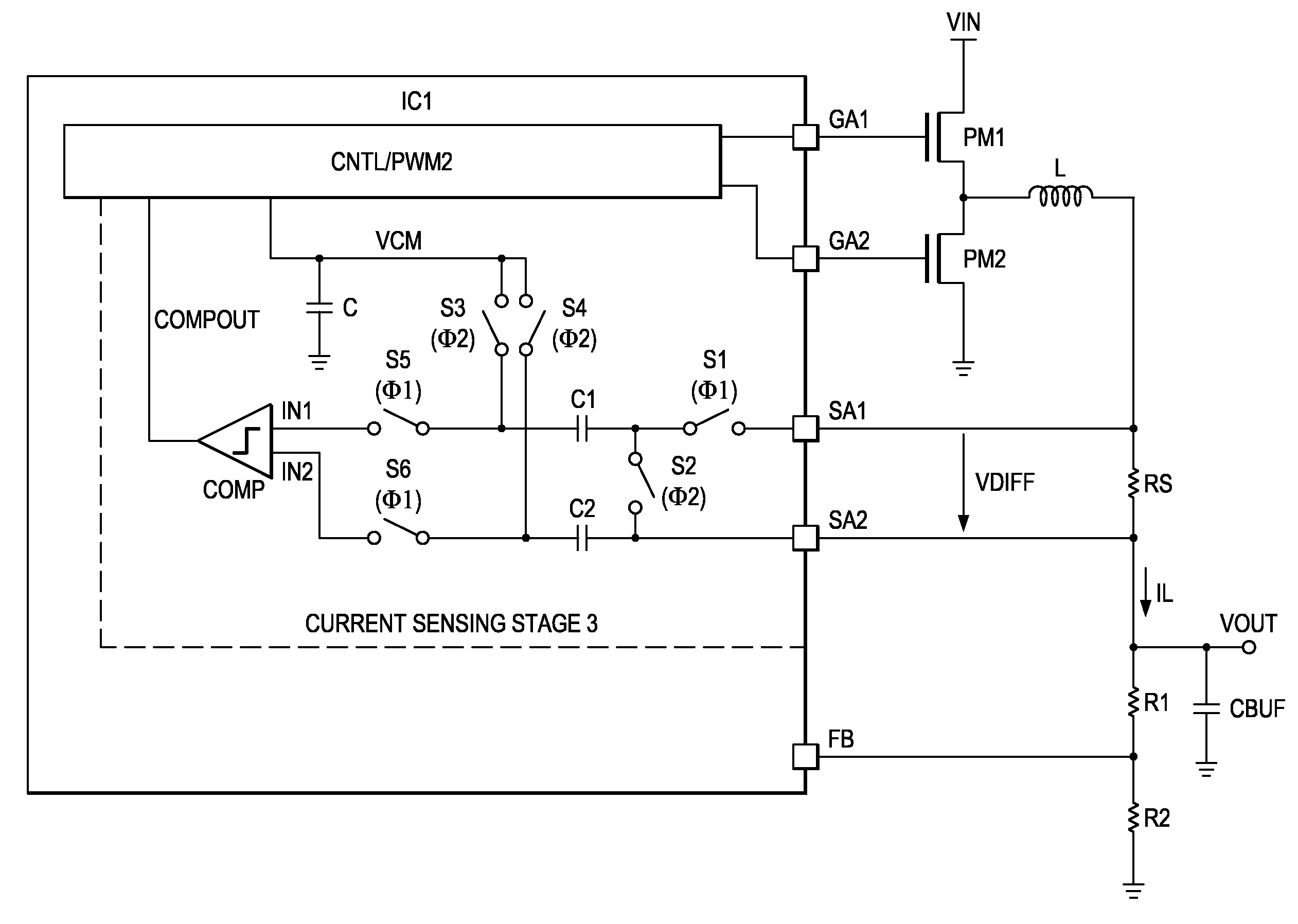
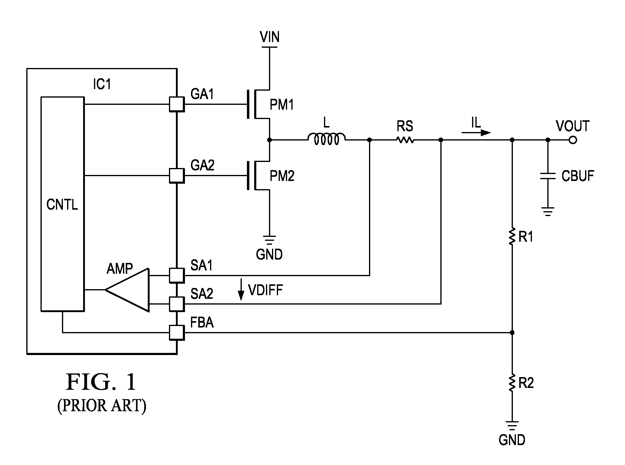
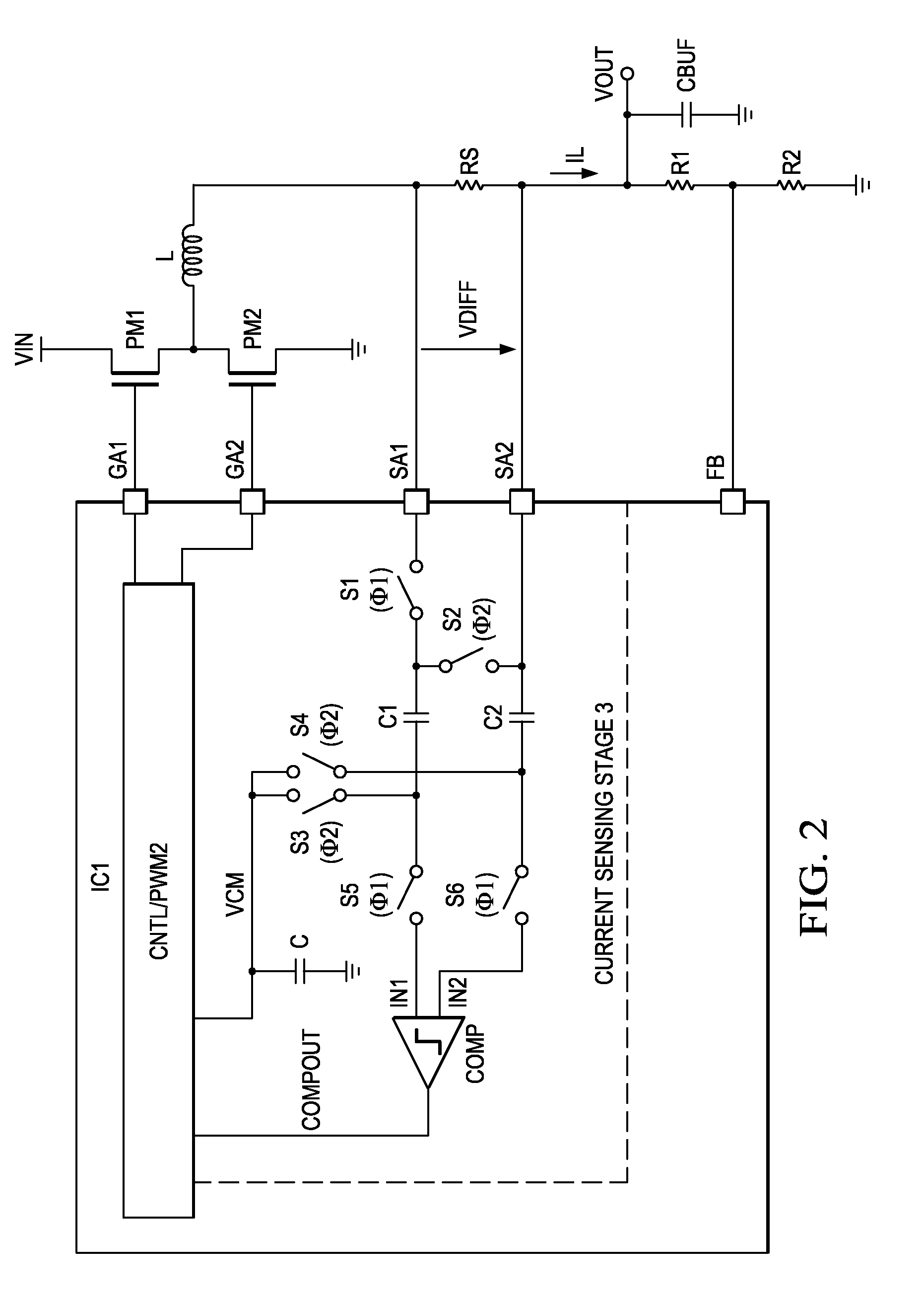
[0032]FIG. 2 shows a simplified circuit diagram of an embodiment of the invention. As described with respect to FIG. 1, control stage CNTL provides control signals for switching power MOSFETs PM1 and PM2 ON and OFF. An output voltage VOUT is generated on an output node and may be buffered with a buffer capacitor CBUF. A shunt resistor RS is coupled into the output path. A load current IL which is supplied from the inductor L to the output node VOUT may then cause a voltage drop across shunt resistor RS. There is a voltage difference VDIFF between nodes SA1 and SA2 which may be input pins of the integrated circuit 1. The current sensing stage 3 includes capacitively coupled comparator COMP. A first input IN1 and a second input IN2 of the comparator COMP are now selectively and capacitively coupled to nodes SA1 and SA2. Comparator COMP detects a magnitude of the voltage difference and / or a relationship between the voltage levels on the first node SA1 and the second node SA2 and provid...


PUM


Abstract

An electronic device for switched mode DC-DC conversion is provided that includes a stage for sensing an output current causing a voltage difference between a first and a second node. The current sensing stage includes a comparator being capacitively coupled with a first input to the first node and with a second input to the second node for determining a magnitude of the output current.

Description

CROSS-REFERENCE TO RELATED APPLICATIONS[0001]This patent application claims priority from German Patent Application No. 10 2009 012 767.4, filed Mar. 12, 2009, which is incorporated herein by reference in its entirety.FIELD OF THE INVENTION[0002]The invention relates to an electronic device and a method for switched mode DC-DC conversion, and more specifically to buck, boost or buck / boost DC-DC converters and a method for operating a buck, boost or buck / boost DC-DC converter.BACKGROUND OF THE INVENTION[0003]DC-DC converters configured as boost or buck or buck / boost converters can use voltage or current sensing modes for determining the magnitude of an output voltage or an output current. In a current sensing mode, the DC-DC converter may sense an output current with a shunt resistor which is coupled in series into an output path. The output current causes a voltage drop across the shunt resistor. The terminals of the shunt resistor are connected to an amplifier the output signal of ...

Claims


Application Information

Patent Timeline
Patent Type & Authority Applications(United States)
IPC IPC(8): G05F1/46
CPCG01R19/0092H02M2001/0009H02M3/156H02M1/0009
Inventor WICHT, BERNHARDKULKARNI, SUMEET P.HERZER, STEFANNEIDHARDT, JOCHEN
Owner TEXAS INSTR INC
Why Eureka
Try Eureka