

Display device
a display device and active matrix technology, applied in the field of display devices, can solve the problems of increasing the number of source lines, and achieve the effects of reducing electric resistance, increasing the aperture ratio, and increasing the line width of the respective storage capacitor wirings
- Summary
- Abstract
- Description
- Claims
- Application Information
AI Technical Summary
Benefits of technology
Problems solved by technology
Method used
Image

Examples
embodiment 1
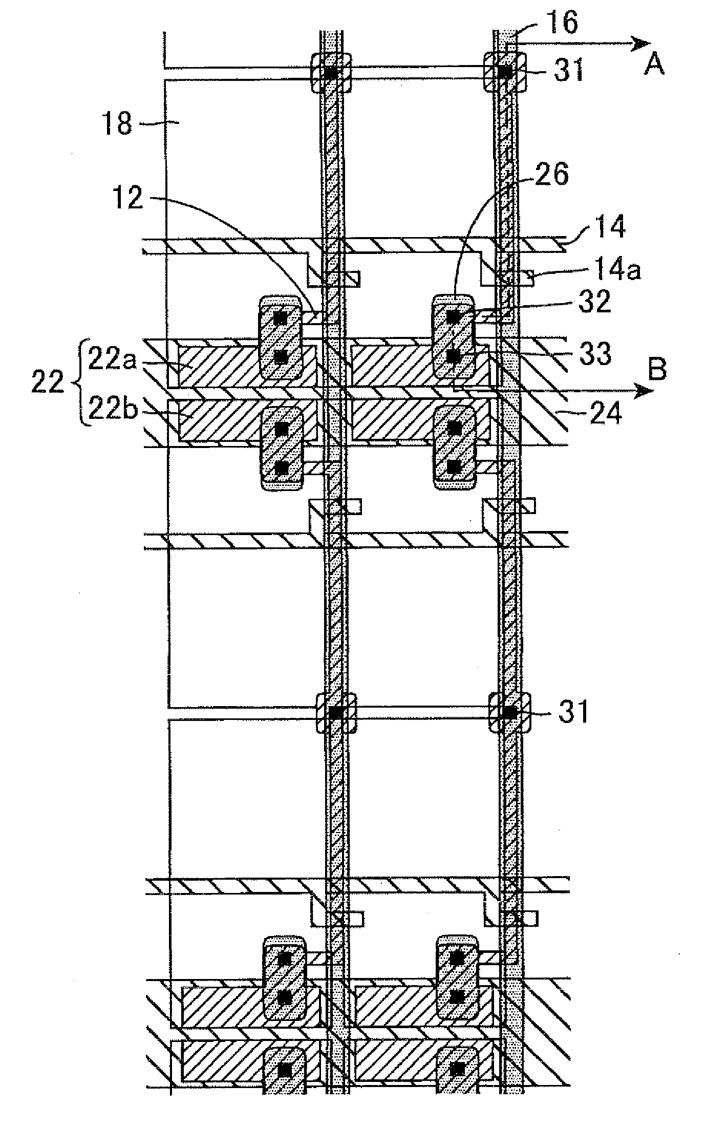
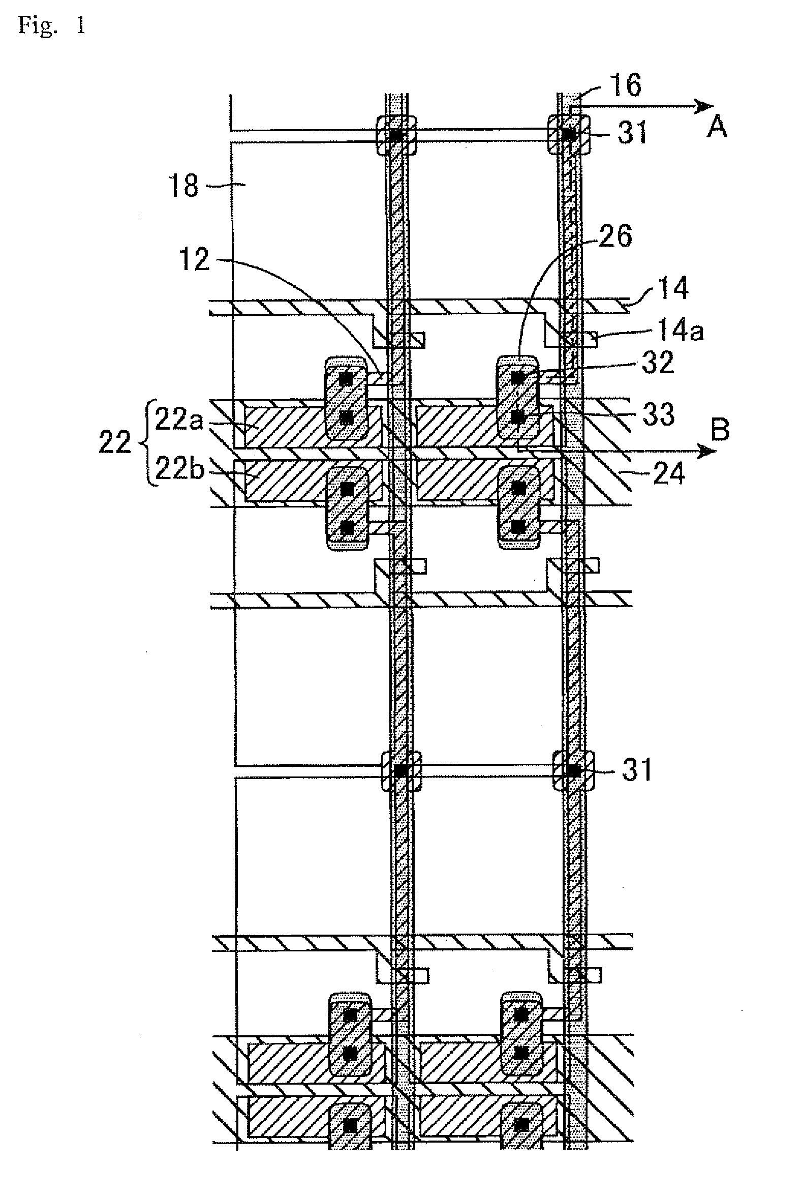
[0038]A liquid crystal display device includes a liquid crystal display panel having a liquid crystal layer between a pair of substrates. Such a device provides display by applying a voltage to the liquid crystal layer from electrodes arranged on the substrates, thereby changing alignment of liquid crystal molecules. According to the present Embodiment, driving of pixels is controlled on an active matrix substrate where TFTs (thin film transistors) and pixel electrodes are arranged in respective pixels in a matrix pattern. FIG. 1 is a plan view schematically showing a circuit configuration of pixels on an active matrix substrate in a display device of Embodiment 1. FIG. 2 is a schematic cross-sectional view taken along line A-B of FIG. 1.
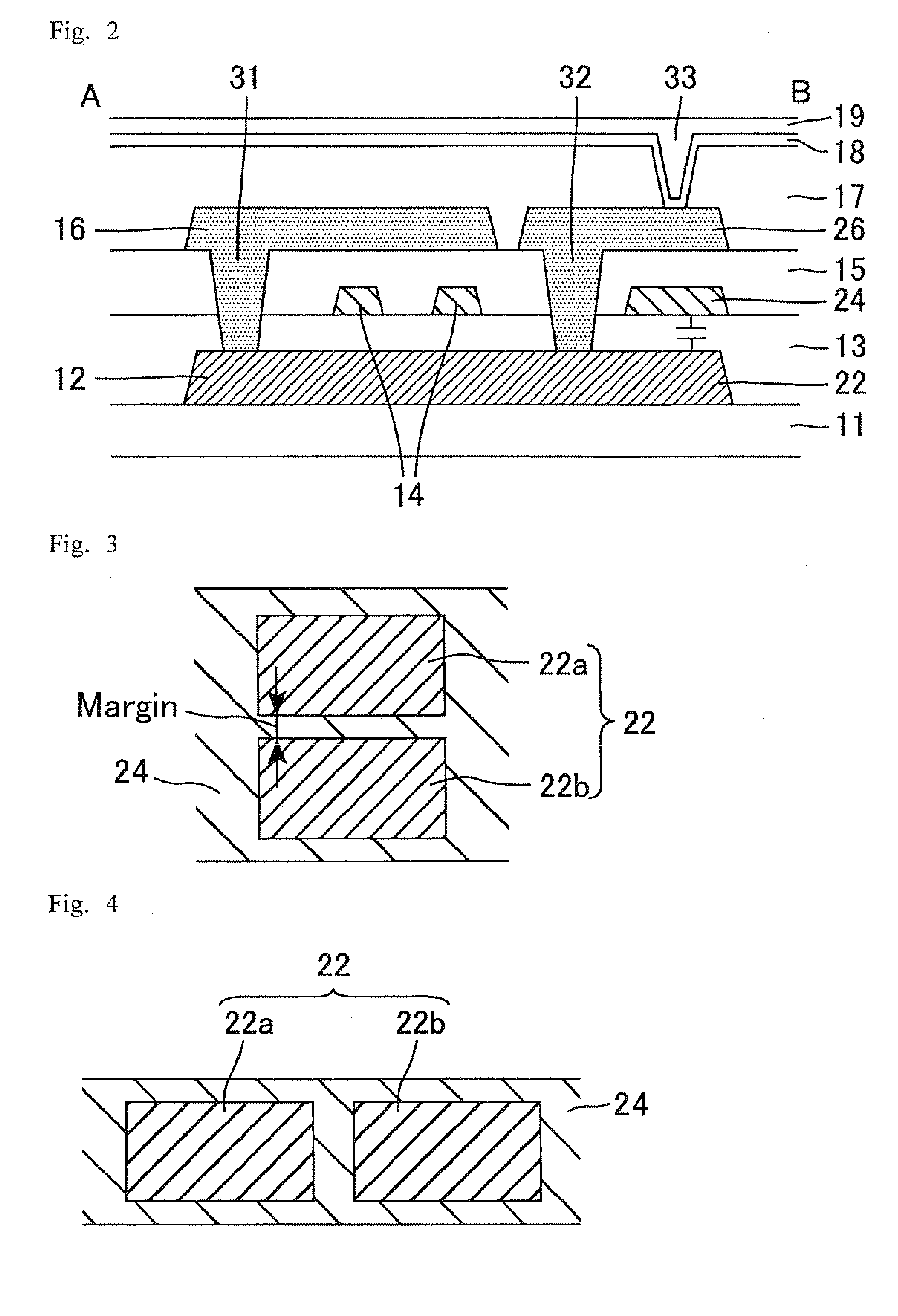
[0039]As shown in FIG. 1, a TFT and a pixel electrode 18 are arranged in respective pixels on the active matrix substrate. The TFT has a portion that is connected to a source line 16 through a first contact hole 31 on one side of a portion where a T...
embodiment 2
[0047]The present Embodiment relates to an embodiment where a storage capacitor wiring is arranged in a boundary region between pixels in an odd-numbered row (Nth row) and pixels in an even-numbered row (N+1th row), and an additional circuit is arranged between the pixels in the even-numbered row (N+1th row) and pixels in the next even-numbered row (N+2th row). FIG. 6 is a schematic plan view of a circuit configuration of pixels, represented by circuit symbols, on an active matrix substrate in a display device in accordance with Embodiment 2. CsL (N, N+1) represents a storage capacitor wiring for driving pixels in the Nth and N+1th rows; GL(N) and GL (N+1) represent gate lines for driving pixels in the Nth and N+1th rows, respectively; SL (M) SL(M+1), and SL (M+2) represent source lines for driving pixels in the Mth, M+1th, and M+2th rows, respectively.
[0048]In the present Embodiment, in a boundary region between the pixels, where no storage capacitor wiring is arranged, a part of a...
embodiment 3
[0055]The present Embodiment relates to a semi-transmissive liquid crystal display device. FIG. 7 is a plan view schematically showing a configuration of pixels in the display device of Embodiment 3. FIG. 8 is a schematic cross-sectional view of liquid crystal display panel taken along line C-D of FIG. 7. According to an active matrix substrate of the semi-transmissive liquid crystal display device of the present Embodiment, a pixel electrode 18 is composed of a transmissive electrode 52 which transmits light and a reflective electrode 53 which reflects light that enters from the liquid crystal layer side. The reflective electrode 53 is arranged at one end of a region where the transparent electrode 52 is arranged. The region where the reflective electrode 53 is arranged is a reflective region. The region where no reflective electrode 53 is arranged within the pixel electrode 18 is a transmissive region. In the present Embodiment, as shown in FIGS. 7 and 8, a configuration of pixels...
PUM
 Abstract
Description
Claims
Application Information