Electronic Device, And Method of Operating An Electronic Device

a technology of electronic devices and flash memory, applied in the field of electronic devices, can solve the problems of local temperature increase, amorphous phase, and flash memory scaling beyond 45 nm nodes,

Active Publication Date: 2010-09-23
NXP BV
View PDF4 Cites 39 Cited by
  • Summary
  • Abstract
  • Description
  • Claims
  • Application Information

AI Technical Summary

Benefits of technology

[0023]It is an object of the invention to provide an electronic component having a convertible structure that can be heated without a demand for high electric power.

Problems solved by technology

In the field of non-volatile memories, flash memory scaling beyond a 45 nm node has become a real issue.
Very high temperatures with rapid cooling down will result in an amorphous phase.
A high current density may lead to a local temperature increase.
Conventionally operated phase change memory cells are therefore large due to the necessity of large transistors and are prone to failure since large programming currents are required.
However, the high power demand of the electric heating procedure according to EP 1,233,418 A1 may be problematic.

Method used


Image

  • Electronic Device, And Method of Operating An Electronic Device
  • Electronic Device, And Method of Operating An Electronic Device
  • Electronic Device, And Method of Operating An Electronic Device

Examples


Embodiment Construction

[0114]The illustration in the drawing is schematical. In different drawings, similar or identical elements are provided with the same reference signs.

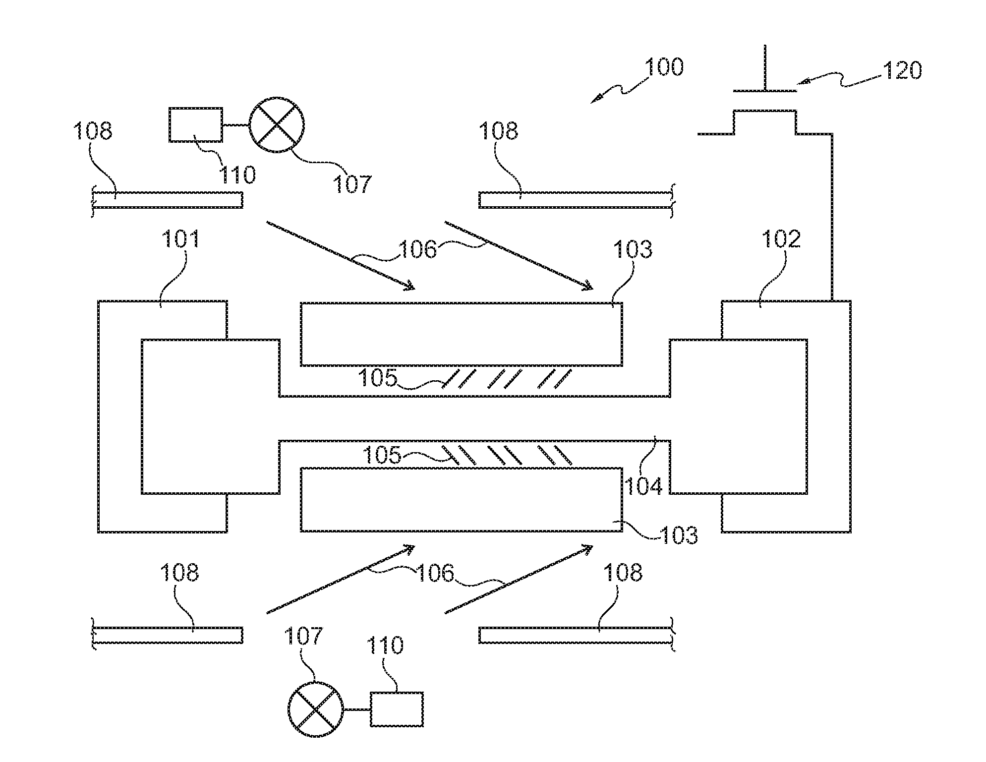
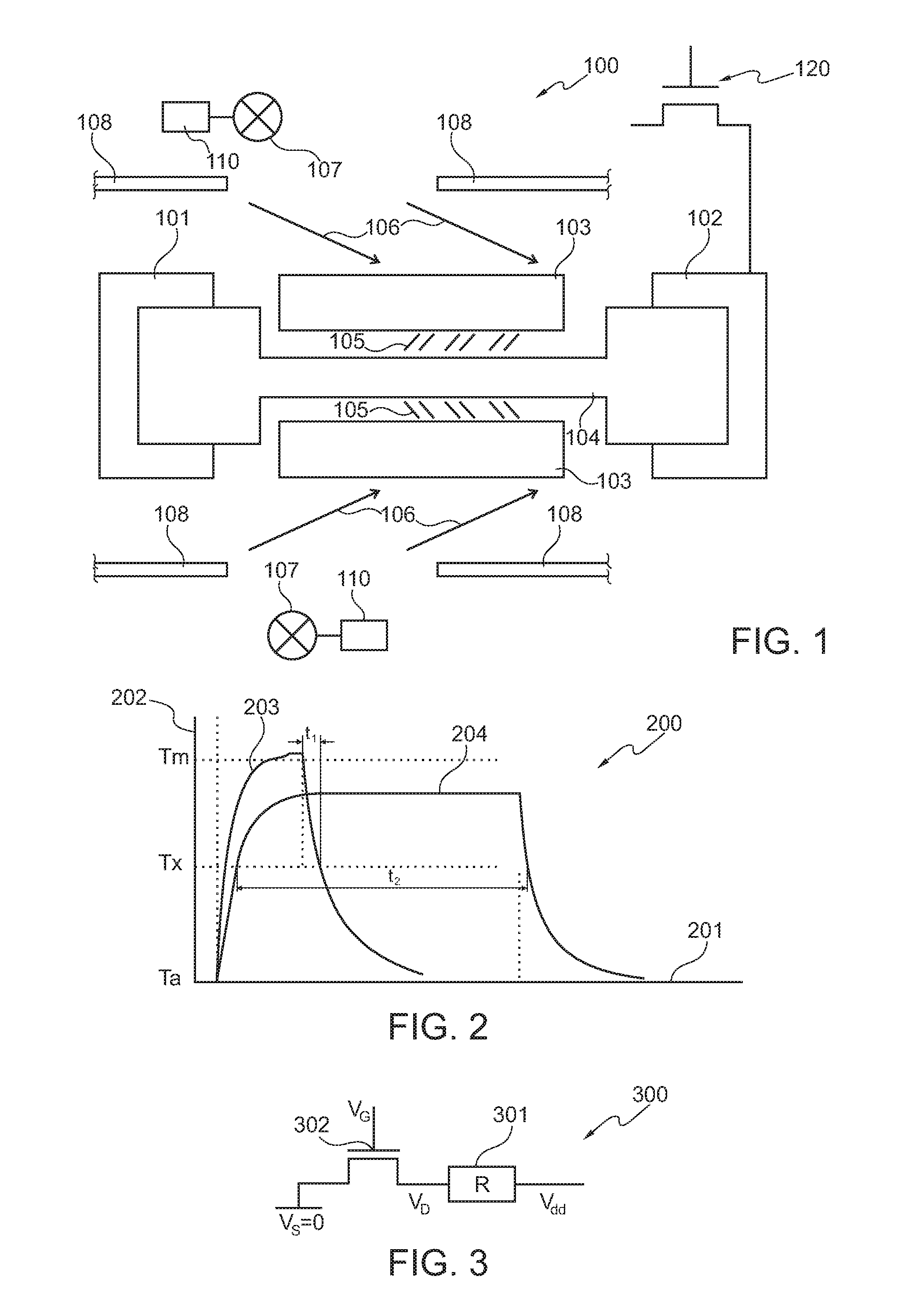
[0115]In the following, referring to FIG. 1, a memory cell 100 as an example for an electronic device according to an exemplary embodiment of the invention will be explained.

[0116]The memory cell 100 comprises a first electrical contact 101 (which may be brought to a reference potential) and a second electrical contact 102. An electrode 103 is provided as a heat transfer structure. A phase change structure 104 made of a chalcogenide material is connected between the first electrical contact 101 and the second electrical contact 102. The chalcogenide 104 is convertible between a crystalline phase and an amorphous phase by heating. In these two states, the electrical conductivity of the phase change structure 104 is different.

[0117]The second electrical contact 102 is coupled to a drain of a switch transistor 120. By applying an appropri...


PUM


Abstract

An electronic device (100) comprising a heat transfer structure (103) and a phase change structure (104) which is convertible between two phase states by heating, wherein the phase change structure (104) is electrically conductive in at least one of the two phase states, wherein the heat transfer structure (103) is arranged to be heated by radiation (106) impinging on the heat transfer structure (103), wherein the phase change structure (104) is thermally coupled to the heat transfer structure (103) so that the phase change structure (104) is convertible between the two phase states when the radiation (106) impinges on the heat transfer structure (103).

Description

FIELD OF THE INVENTION[0001]The invention relates to an electronic device.[0002]Moreover, the invention relates to a method of operating an electronic device.BACKGROUND OF THE INVENTION[0003]In the field of non-volatile memories, flash memory scaling beyond a 45 nm node has become a real issue. Technologies to face this challenge are ferroelectric, magnetic and phase change memories, the latter one being promising for the replacement of flash and showing characteristic that may allow replacement of other types of memories such as DRAM. Phase change memories are a possible solution for the unified memory being an important step in the electronics art. OTP (“on time programmable”) and MTP (“multiple times programmable”) memories open a field that may present a great opportunity for phase change memories as well.[0004]Phase change memories are based on a reversible memory switching using, for instance, chalcogenide materials. Thus, phase change materials may be used to store informatio...

Claims


Application Information

Patent Timeline
Patent Type & Authority Applications(United States)
IPC IPC(8): G11C11/00H01L45/00
CPCH01L45/06H01L45/1286H01L45/1226H10N70/823H10N70/231H10N70/8613
Inventor TIO CASTRO, DAVIDATTENBOROUGH, KAREN
Owner NXP BV
Why Eureka
Try Eureka