Methods of making an emitter having a desired dopant profile

a technology of dopant profile and emitter, which is applied in the manufacture of final products, basic electric elements, coatings, etc., can solve the problems of difficult gas source handling, difficult gaseous diffusion process, and breakage of silicon substrates, and achieve the effect of avoiding the formation of prior art junction formation techniques and not being economical for solar cell fabrication

Inactive Publication Date: 2010-09-23
APPLIED MATERIALS INC
View PDF12 Cites 71 Cited by
  • Summary
  • Abstract
  • Description
  • Claims
  • Application Information

AI Technical Summary

Benefits of technology

[0012]Embodiments of the present invention further provide a method for forming a selective emitter for a silicon solar cell in a crystalline silicon substrate, comprising depositing a first amorphous silicon layer doped with phosphorous at a first doping level on a first surface of the crystalline silicon substrate, heating a second surface of the crystalline silicon substrate with a temperature gradient across the crystalline silicon substrate to cause solid phase epitaxial crystalliza...

Problems solved by technology

Such handling of the substrates inevitably results in breakage of some of the silicon substrates since they are relatively thin, being on the order of 0.3 mm thick or less.
Although phosphorous diffusion of the phosphorous doped n-type silicon material for solar junction formation could be created by the furnace type diffusion/annealing processes as discussed above, these processes require handling of gaseous...

Method used


Image

  • Methods of making an emitter having a desired dopant profile
  • Methods of making an emitter having a desired dopant profile
  • Methods of making an emitter having a desired dopant profile

Examples


Embodiment Construction

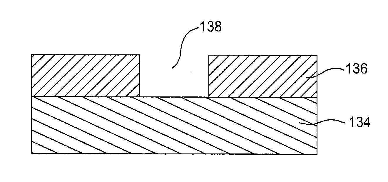
[0023]The present invention provides a method for obtaining a desired emitter doping profile by depositing layers of amorphous silicon on a surface of a crystalline silicon substrate. The amorphous silicon, when it is deposited on the crystalline silicon substrate, may, in accordance with one embodiment of the present invention, be doped with doping material of the opposite conductivity type of the silicon substrate so as to provide a p-n junction when a doping material in the amorphous silicon has been diffused into the crystalline silicon substrate. For example, if the crystalline silicon substrate is formed of p-type silicon material, then the deposited amorphous silicon layer would be doped with phosphorous atoms to provide an n-type emitter layer on the surface of the crystalline silicon substrate. Either one or two layers of amorphous silicon are deposited on the silicon substrate. If two layers of amorphous silicon are deposited on the substrate, then the first layer may be l...


PUM

PropertyMeasurementUnit
Temperatureaaaaaaaaaa

Abstract

A method for obtaining a desired dopant profile of an emitter for a solar cell which includes depositing a first amorphous silicon layer having a first doping level over an upper surface of the crystalline silicon substrate, depositing a second amorphous silicon layer having a second doping level on the first amorphous silicon layer, and heating the crystalline silicon substrate and the first and second amorphous silicon layers to a temperature sufficient to cause solid phase epitaxial crystallization of the first and second amorphous silicon layers, such that the first and second amorphous silicon layers, after heating, have the same grain structure and crystal orientation as the underlying crystalline silicon substrate

Description

CROSS-REFERENCE TO RELATED APPLICATIONS[0001]This application claims benefit of U.S. Provisional Patent Application Ser. No. 61 / 098,713 [Attorney Docket #: APPM 12138L], filed Sep. 19, 2008, and Provisional Patent Application Ser. No. 61 / 098,718 [Attorney Docket #: APPM 12139L], filed Sep. 19, 2008, which are both herein incorporated by reference in their entirety.FIELD OF THE INVENTION[0002]This invention relates generally to silicon solar cells and, more particularly, to a method for obtaining a desired dopant profile in the emitter of a solar cell device. The method allows for any desired profile of dopant in the emitter to maximize the cell performance.DESCRIPTION OF THE RELATED ART[0003]Solar cells are material junction devices which convert sunlight into direct current (DC) electrical power. Solar cells typically have one or more p-n junctions. Each junction comprises two different regions within a semiconductor material where one side is denoted as the p-type region and the o...

Claims


Application Information

Patent Timeline
IPC IPC(8): H01L31/18
CPCH01L21/02532H01L21/02573H01L21/02667H01L31/022425Y02E10/547H01L31/068H01L31/1872Y02E10/52H01L31/03529H01L31/022441H01L31/0682Y02P70/50
Inventor RANA, VIRENDRA V.S.BACHRACH, ROBERT Z.
Owner APPLIED MATERIALS INC
Why Eureka
Try Eureka