

Method of forming semiconductor device having a capacitor
a technology of capacitors and semiconductor devices, which is applied in the direction of capacitors, semiconductor devices, electrical equipment, etc., can solve the problems of capacitor electrical characteristics degrading, and high aspect ratio of electrodes, and achieve the effect of preventing surface contamination of capacitor electrodes
- Summary
- Abstract
- Description
- Claims
- Application Information
AI Technical Summary
Benefits of technology
Problems solved by technology
Method used
Image

Examples
first example embodiment
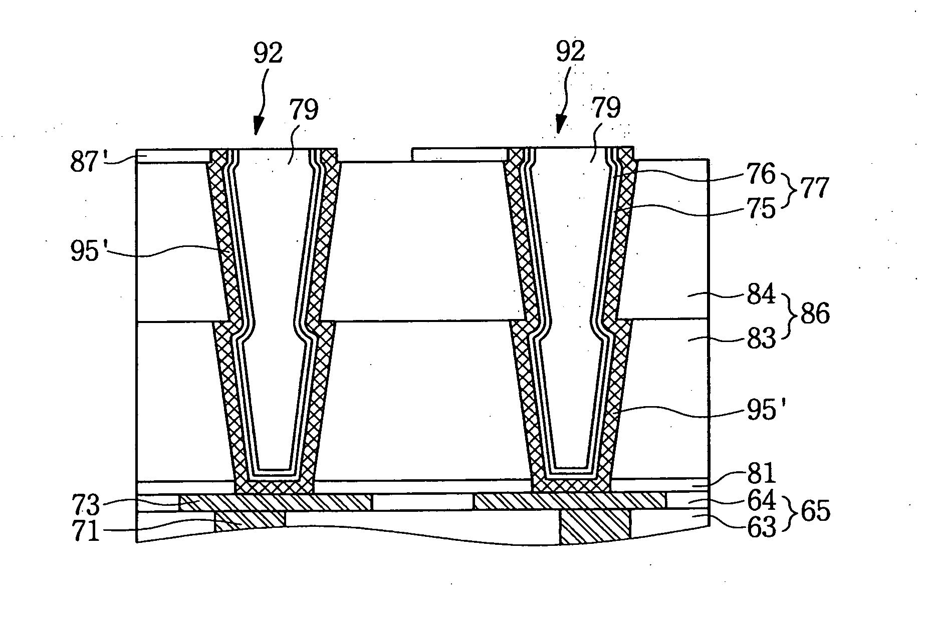
[0032]FIGS. 2-4, 6, 8, 9, 11, and 13 illustrate cross-sectional views of stages in a method of forming a semiconductor device having a capacitor according to a first example embodiment. FIG. 5 illustrates a detailed view of E1 of FIG. 4, FIG. 7 illustrates a detailed view of E2 of FIG. 6, and FIG. 12 illustrates a detailed view of E3 of FIG. 11. FIG. 10 illustrates a plan view for assisting understanding of FIG. 9.
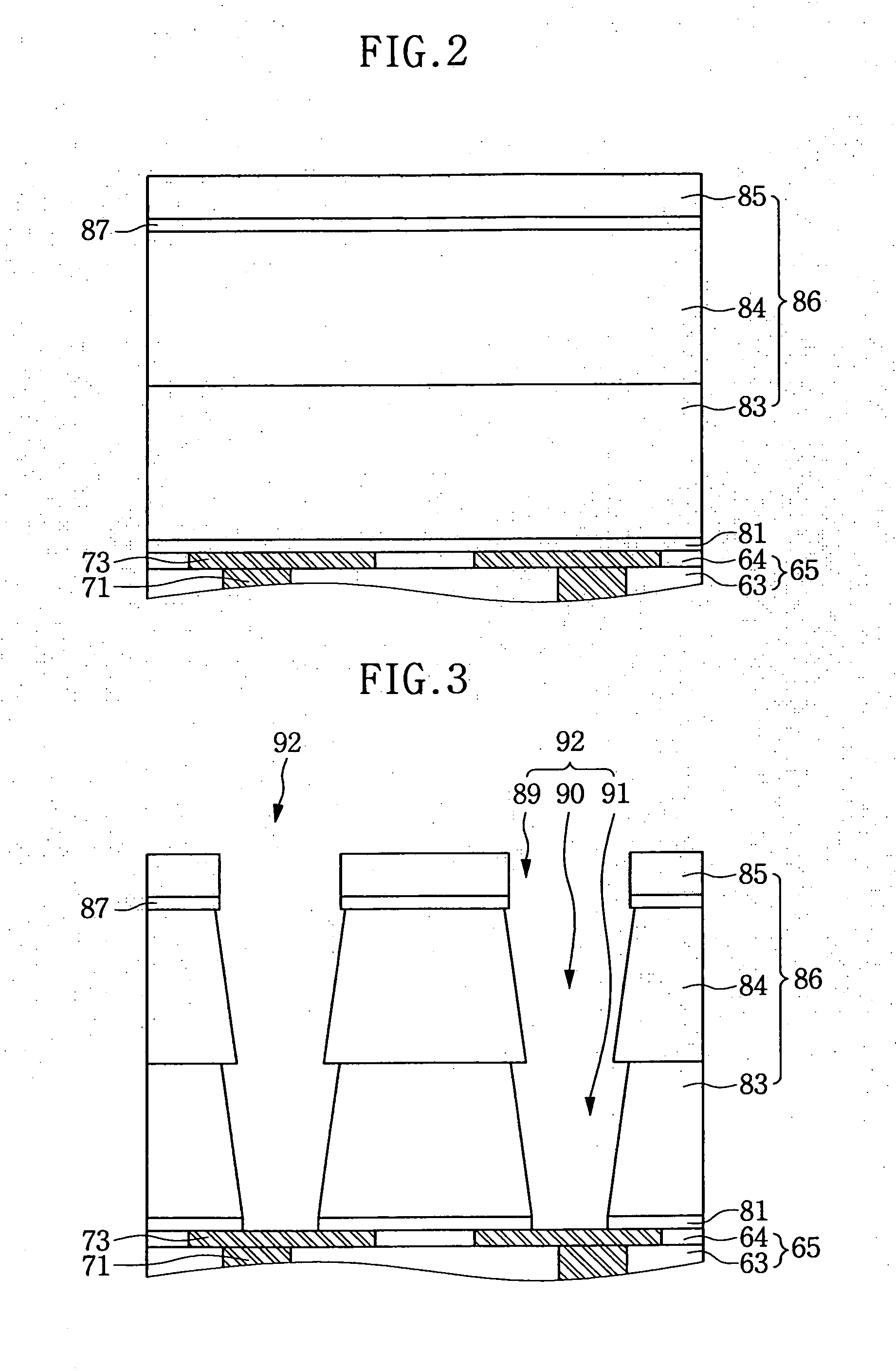
[0033]Referring to FIG. 2, a lower insulating layer 65, a buried contact plug 71, and a landing pad 73 may be formed on a substrate (not shown). The lower insulating layer 65 may include a first insulating layer 63 covering the substrate and a second insulating layer 64 covering the first insulating layer 63. The lower insulating layer 65 may be formed, e.g., of a silicon oxide layer, a silicon nitride layer, a silicon oxynitride layer and / or a combination thereof.
[0034]The buried contact plug 71 may penetrate the first insulating layer 63. The landing pad 73 may penetrate...
second example embodiment
[0063]FIGS. 14 to 20 illustrate cross-sectional views of stages in a method of forming a semiconductor device having a capacitor according to a second example embodiment.
[0064]Referring to FIG. 14, the lower insulating layer 65, the buried contact plug 71 and the landing pad 73 may be formed on the substrate (not shown). The lower insulating layer 65 may include the first insulating layer 63 and the second insulating layer 64. The landing pad 73 and the buried contact plug 71 may be formed in plural number to be, e.g., regularly, arranged in row and column directions. The landing pads 73 may be omitted.
[0065]The etch stop layer 81 and a molding layer 186 may be sequentially formed on the substrate having the lower insulating layer 65 and the landing pads 73 (S10 of FIG. 1).
[0066]The molding layer 186 may be formed of a material layer having a higher etch rate than the etch stop layer 81. For example, a ratio of an etch rate of the molding layer 186 to an etch rate of the etch stop l...
third example embodiment
[0083]FIG. 21 illustrates a cross-sectional view of a method of forming a semiconductor device having a capacitor according to a third example embodiment. The method may be substantially the same as the second exemplary embodiment, with the exception of having only the first oxide layer 175 as a surface oxide layer.
[0084]Referring to FIG. 21, the lower insulating layer 65, the buried contact plug 71, and the landing pad 73 may be formed on the substrate (not shown). The lower insulating layer 65 may include the first insulating layer 63 and the second insulating layer 64. The landing pad 73 and the buried contact plug 71 may be formed in plural number to be regularly arranged in row and column directions. The landing pad 73 may be omitted. Only a difference from the second example embodiment will be briefly described below.
[0085]The etch stop layer 81 and the molding layer 186 may be sequentially formed on the substrate having the lower insulating layer 65 and the landing pads 73 (S...
PUM
| Property | Measurement | Unit |
|---|---|---|
| aspect ratio | aaaaa | aaaaa |
| thickness | aaaaa | aaaaa |
| thickness | aaaaa | aaaaa |
Abstract
Description
Claims
Application Information