Solar cell and fabrication method thereof

a solar cell and fabrication method technology, applied in the field of solar cells, can solve the problems that commercialized bulk silicon solar cells have not been widely used, and achieve the effects of excellent light trapping capability, excellent efficiency, and improved contact resistance between metal and silicon

Inactive Publication Date: 2010-09-30
LG ELECTRONICS INC
View PDF13 Cites 85 Cited by
  • Summary
  • Abstract
  • Description
  • Claims
  • Application Information

AI Technical Summary

Benefits of technology

[0060]With the solar cell and the fabrication method thereof according to the present invention, a solar cell having the excellent light trapping capability, improved contact resistance between metal and silicon, and excellent efficiency while reducing the loss caused by the recombination of electrons and holes can be provided, as compared to a crystalline silicon solar cell according to t...

Problems solved by technology

In recent years, new forms of renewable energy are of much interest due to problems, such as rising oil prices, global warming, exhaustion of fossil energy, nuclear waste disposal, position selecti...

Method used


Image

  • Solar cell and fabrication method thereof
  • Solar cell and fabrication method thereof
  • Solar cell and fabrication method thereof

Examples


Embodiment Construction

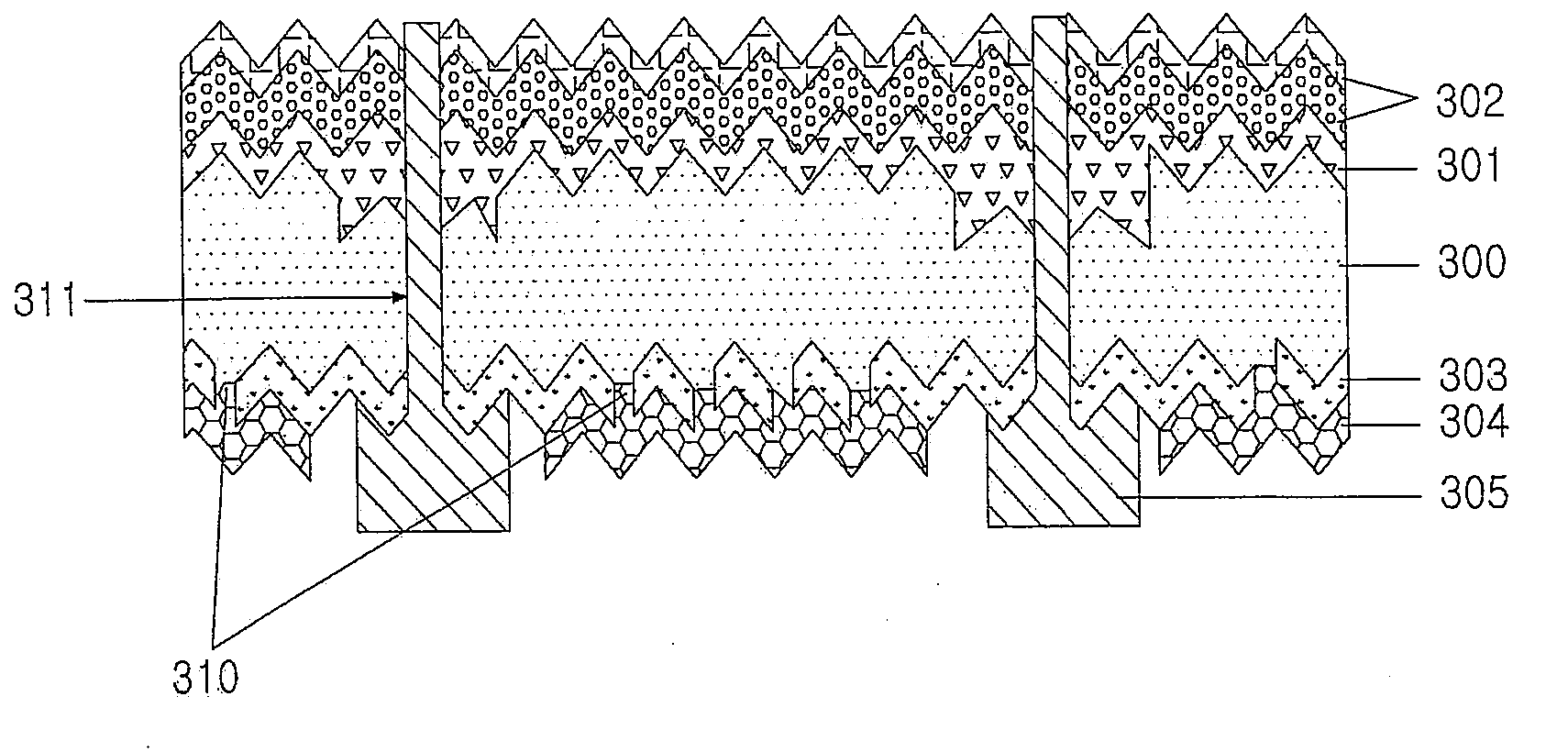
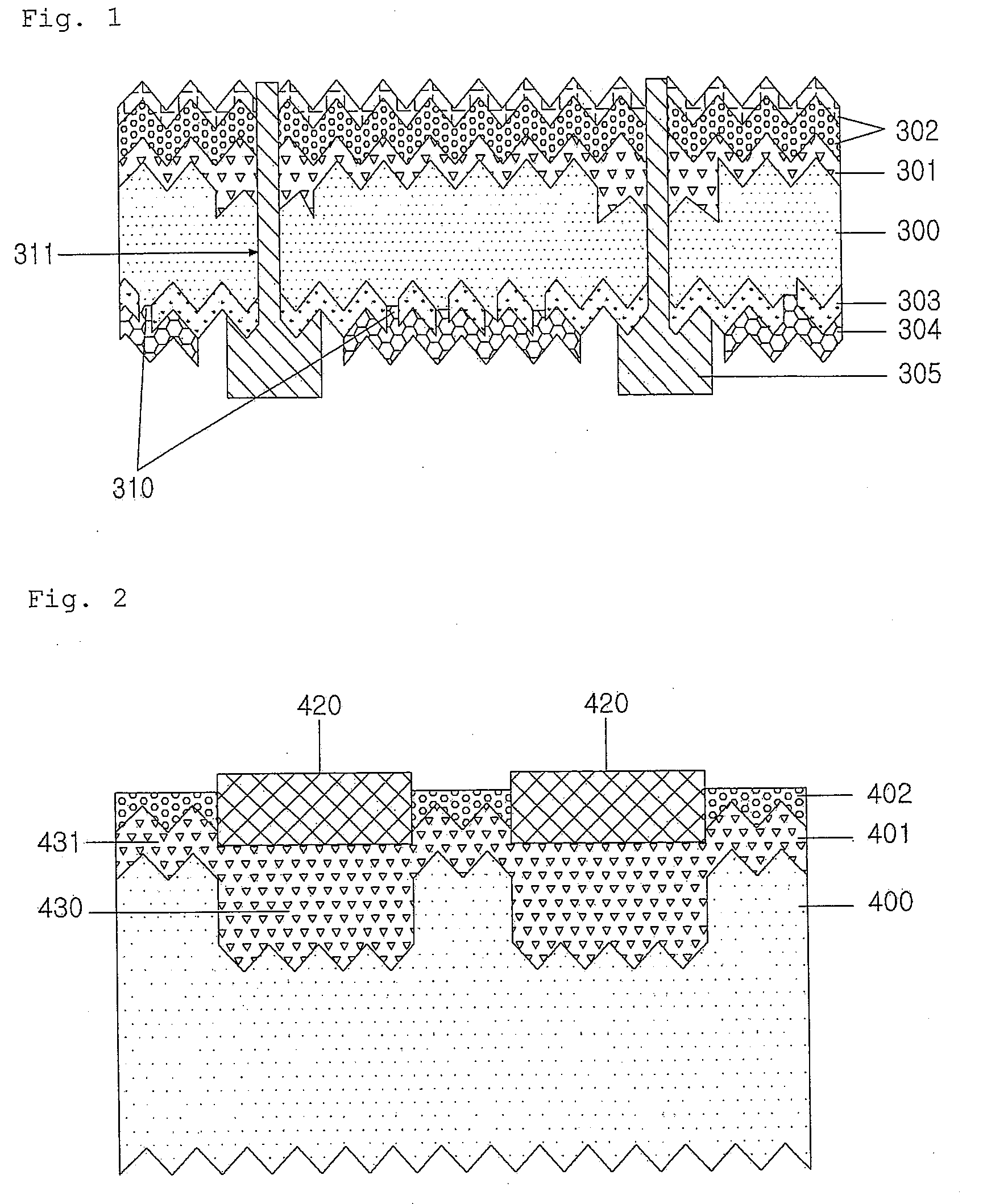
[0067]FIG. 1 is a cross-sectional view of a solar cell according to one embodiment of the present invention. Hereinafter, a structure of the solar cell of the present invention will be described with reference to FIG. 1.

[0068]The solar cell of the present invention comprises a semiconductor substrate 300, an emitter layer 301 that is formed on a front surface (a light incident surface or an upper surface) and a side surface of the semiconductor substrate, or the front surface, the side surface, and a rear surface (a back surface or a lower surface) of the semiconductor substrate, a passivation layer 303 that is formed on the rear surface of the semiconductor substrate, at least one localized back surface field (BSF) layer 304 that is formed at a predetermined portion on the passivation layer and connected with the semiconductor substrate, and a metal electrode 305 that penetrates through the front surface and rear surface of the semiconductor substrate.

[0069]The front surface of the...


PUM


Abstract

Disclosed are a metal wrap through solar cell including a metal wrap through (MWT) structure as a back contact silicon solar cell and a fabrication method thereof.

Description

[0001]This application claims priority to Korean Patent Application No. 10-2009-0025462, filed on Mar. 25, 2009, in the Korean Intellectual Property Office, the entire contents of which are hereby incorporated by reference.BACKGROUND OF THE INVENTION[0002]1. Field of the Invention[0003]The present invention relates to a solar cell and a fabrication method thereof, and in particular, to a metal wrap through solar cell including a metal wrap through (MWT) structure as a back contact silicon solar cell and a fabrication method thereof. More specifically, the present invention relates to a solar cell capable of increasing the efficiency of a solar cell by leaving only a metal finger line on a front surface of the solar cell and installing a metal electrode on a rear surface of a semiconductor substrate by penetrating through the semiconductor substrate, instead of a solar cell wherein a bus bar electrode is formed on a front surface of a solar cell according to the related art, and a fa...

Claims


Application Information

Patent Timeline
IPC IPC(8): H01L31/0224H01L31/18
CPCH01L31/02168H01L31/02245H01L31/068H01L31/1804H01L31/022458Y02E10/547H01L31/0684H01L31/0682Y02E10/52Y02P70/50
Inventor KIM, JONG-HWAN
Owner LG ELECTRONICS INC
Why Eureka
Try Eureka