Soldering Method and Related Device for Improved Resistance to Brittle Fracture

a technology of brittle fracture and soldering method, which is applied in the field of soldering, can solve the problems of limited stress on the joint, unsatisfactory thermal loading effect, and joints that are more susceptible to brittle failure than joints, and achieve the effect of improving the solder joint and less prone to brittle failur

Active Publication Date: 2010-09-30
BELL SEMICON LLC
View PDF9 Cites 27 Cited by
  • Summary
  • Abstract
  • Description
  • Claims
  • Application Information

AI Technical Summary

Benefits of technology

[0010]In one aspect, an electronic device is disclosed that has an improved solder joint that is less prone to brittle failure. In one embodiment, an electronic device comprises a non-conductive core layer, one or more conductive copper (Cu) layers, one or more polymer insulating layers, a polymer layer over the outer-most Cu layer with openings to expose Cu regions referred to as pads, a nickel (Ni) layer disposed over at least a portion of the exposed Cu pads, a gold (Au) layer deposited on top of the Ni layer, and an intermetallic compound (IMC) region that couples the solder mass to the Ni layer. The Ni and Au layers contain no more than 5000 ppm by weight of phosphorus (P), preferably less than 500 ppm by weight of P, more preferably less than 50 ppm by weight of P, even more preferably less than 10 ppm by weight of P, and more preferably still less than 1 ppm by weight of P.

Problems solved by technology

These higher reflow temperatures can lead to undesirable thermal loading effects including those associated with differential thermal expansion-induced stresses.
Furthermore, the yield point of Pb-free alloys, which essentially puts a limitation on the magnitude of the stress the joint can be exposed to, is more sensitive to the strain rate of the applied stress than for PbSn alloys.
These combined mechanical properties of Pb-free solders tend to make joints that are more susceptible to brittle failure than joints made from PbSn solders.
This is especially true when the joints are exposed to stresses applied at high strain rates, such as those that may occur during testing, handling, and assembly.
Packages that contain solder spheres, typically referred to as solder balls or solder bumps, as part of the overall device electrical interconnect are prone to high strain rate brittle fracture.
This reflow process can be quite intricate, and a detailed discussion is beyond the scope of this disclosure.
Stress imparted to the solder balls 20 during testing, shipping, assembly, accidental dropping or the like may cause the solder balls 20 to separate from their respective pads 11, and thus lead to electrical failure.
Reduction in the Ag content reduces the yield strength of the alloy.
Although some researchers have found low Ag content solders are less prone to brittle failure during drop testing, other data is not as clear.

Method used


Image

  • Soldering Method and Related Device for Improved Resistance to Brittle Fracture
  • Soldering Method and Related Device for Improved Resistance to Brittle Fracture
  • Soldering Method and Related Device for Improved Resistance to Brittle Fracture

Examples


Embodiment Construction

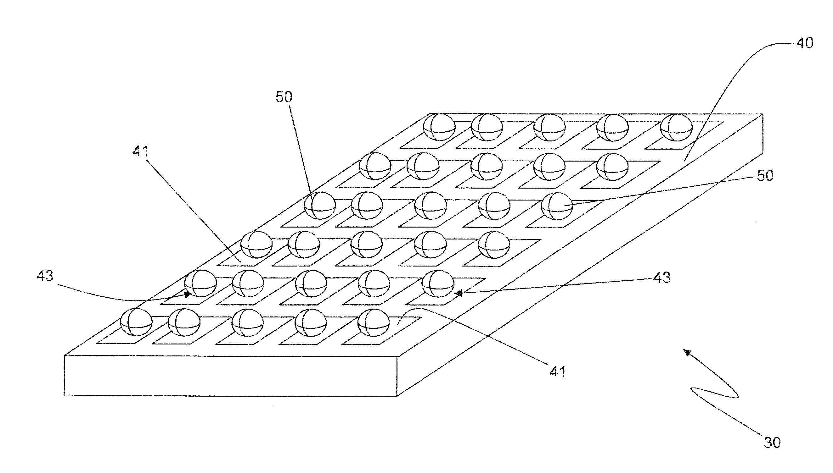
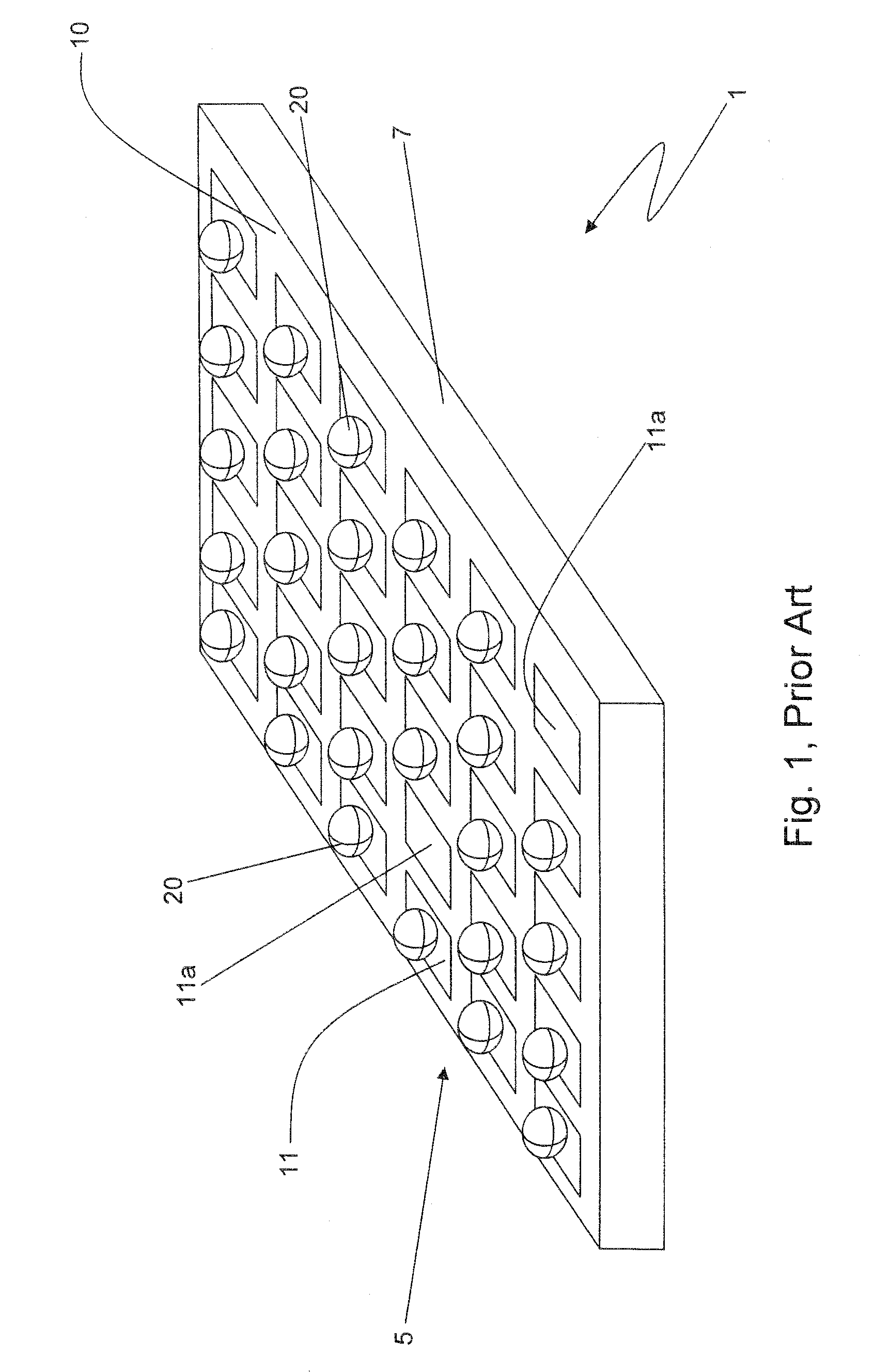
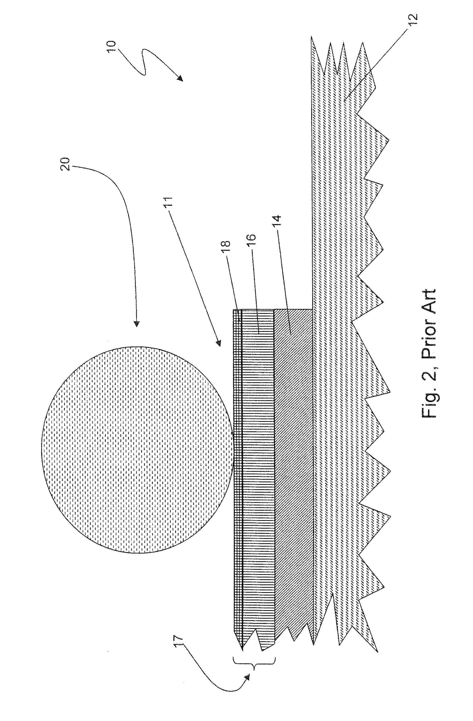
[0027]Soldering methods, and related devices employing solder joints formed according to the soldering methods, are generally described herein. For purposes of the following, an intermetallic compound (IMC) region need not contain only metals, but may also contain other elements in the form of inclusions within the solder itself and within the metal layers with which the solder reacts or contacts. An IMC may be thought of as the reactive region or contact region between the solder and the metal to which the solder binds. Additionally, when a first layer is said to be disposed “over” a second layer or device, it should be understood that the first layer may be disposed on the second layer or device, or may be disposed upon a third layer or layers that are in turned disposed on the second layer or device. The third layer or layers may not be explicitly indicated in the interests of brevity.

[0028]It has been discovered that high strain rate brittle failure occurs in a solder joint with...


PUM

PropertyMeasurementUnit
temperatureaaaaaaaaaa
thicknessesaaaaaaaaaa

Abstract

A lead-free solder joint is formed between a tin-silver-copper solder alloy (SAC), SACX, or other commonly used Pb-free solder alloys, and a metallization layer of a substrate. Interaction of the SAC with the metallization layer forms an intermetallic compound (IMC) that binds the solder mass to the metallization layer. The IMC region is substantially free of any phosphorous-containing layers or regions.

Description

FIELD OF THE INVENTION[0001]The present invention relates generally to soldering. More particularly, the present invention discloses a method for reducing brittle fracture failure rates in joints made with lead-free solders.BACKGROUND OF THE INVENTION[0002]In response to environmental concerns and legislative action, manufacturers of electronic devices are switching from lead-containing (Pb-containing) to lead-free (Pb-free) solders. The transition from Pb-containing to Pb-free solders has not been without problems. The most widely used Pb-free solders in the electronics industry contain a high tin (Sn) content, typically in excess of 94 wt. %, and further contain silver (Ag), copper (Cu), or both, and possibly other elements such as nickel (Ni), cobalt (Co), zinc (Zn), bismuth (Bi), etc. Solder alloys that contain Sn, Ag, and Cu are referred to as SAC solders. If they contain an additional element they are usually referred to as SACX, where X represents the additional element. SAC ...

Claims


Application Information

Patent Timeline
Patent Type & Authority Applications(United States)
IPC IPC(8): H05K1/09B23K31/02B23K1/20
CPCH05K3/244H01L2224/16225H05K3/3463
Inventor AMIN, AHMEDBAIOCCHI, FRANKDELUCCA, JOHNOSENBACH, JOHNVACCARO, BRIAN T.
Owner BELL SEMICON LLC
Why Eureka
Try Eureka