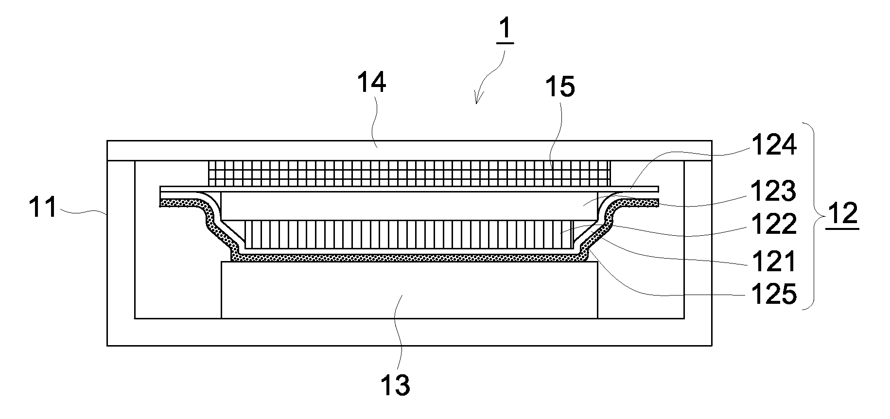
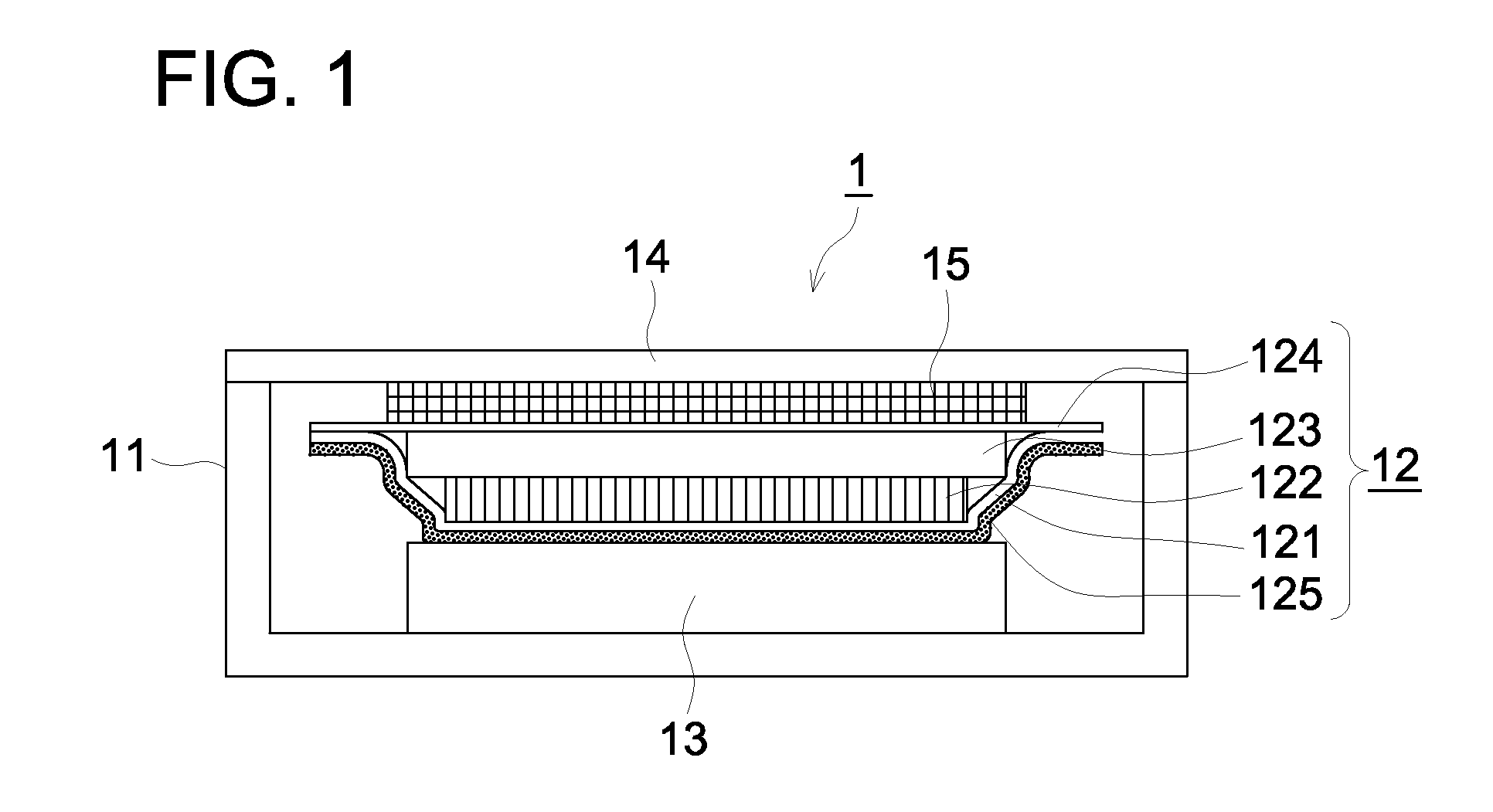
Flat Panel Detector

a detector and flat panel technology, applied in the field of flat panel detectors, can solve the problems of insufficient spatial resolution, insufficient image sharpness, inability to realize free image processing or instantaneous image transfer, etc., and achieve the effect of preventing aging and deterioration of characteristics

Active Publication Date: 2010-09-30
KONICA MINOLTA MEDICAL & GRAPHICS INC
View PDF4 Cites 29 Cited by
  • Summary
  • Abstract
  • Description
  • Claims
  • Application Information

AI Technical Summary

Benefits of technology

[0029]According to the present invention, there can be provided a flat panel detector which prevents aging deterioration of characteristics of a phosphor layer, protects the phosphor layer from chemical alteration or physical impact, and maintains a stable contact state between the scintillator panel and the flat light receiving element.

Problems solved by technology

However, these image data are so-called analog image data, in which free image processing or instantaneous image transfer cannot be realized.
However, image sharpness is insufficient and spatial resolution is also insufficient, which have not yet reached the image quality level of the conventional screen / film system.
A thicker phosphor layer causes more scattering of emission within the phosphor layer, leading to deteriorated sharpness.
However, the use of CsI alone results in reduced emission efficiency.
However, a scintillator (phosphor layer) based on CsI exhibits deliquescence and suffered a disadvantage of characteristics being deteriorated with aging.
In this case, excessively strong pressure of the cushioning material breaks the top portion of phosphor crystals having a columnar crystal structure, resulting in lowered contrast of a radiation image.
To the contrary, in cases of a weak pressure of the cushioning material, a displacement between the scintillator panel surface and the flat light receiving element surface is caused when turning the FPD downward or by vibration, resulting in reduced signal correction precision at the individual elements of a flat light receiving element and leading to deteriorated graininess or sharpness of the obtained image.
There is also produced problems such that friction between a scintillator panel and a flat light receiving element, caused by movement or vibration of the FPD, tends to produce defects in the flat light receiving element or the phosphor layer.
In general, the thickness of a phosphor layer needs to be not less than 400 μm to obtain a radiation image of enhanced graininess; however, the increased mass of the scintillator panel, due to such an increased layer thickness or an increased panel size has pronounced the foregoing problems.
To overcome such problems, there has been proposed a method of securing a scintillator panel and a flat light receiving element with an adhesive (as described in, for example, patent document 1) or a method of pasting them together with a matching oil (as described in, for example, patent document 2), but producing problems such as occurrence of unevenness due to the adhesive or the matching oil, or the increased number of work steps.
Further, overhaul of a FDP or replacement of a scintillator panel is impossible in these methods, producing serious problems in maintenance.
However, formation of a scintillator layer on a substrate which cannot be freely bent is easily affected by deformation of the substrate or curvature at the time of vapor deposition when sticking a scintillator plate on the flat light-receiving element surface with paste, leading to defects such that uniform image quality characteristics cannot be achieved with the flat light-receiving surface of a flat panel detector.
Accordingly, such problems have become serious along with the recent trend of increasingly larger flat panel detectors.

Method used


Image

  • Flat Panel Detector
  • Flat Panel Detector

Examples


examples

[0074]The present invention will be specifically described with reference to examples but is not limited to these. In the examples, expression of “%” represents “% by mass” unless otherwise noted.

example

Preparation of Scintillator Plate

Preparation of Substrate:

[0075]There were prepared 125 μm and 225 μm thick polyimide films (250×300 mm).

Formation of Phosphor Layer:

[0076]Using a vapor deposition apparatus, a phosphor (CsI:0.3% Tl) was formed on prepared polyimide film by a process of vapor deposition to prepare a scintillator, as described below.

[0077]A phosphor raw material (CsI:0.3% Tl) was loaded into a resistance heating crucible, polyimide film was set on a supporting holder, and the distance between the resistance heating crucible and an aluminum plate was adjusted to 400 mm. Subsequently, the interior of the vapor deposition apparatus was evacuated and after argon gas was introduced thereto and the vacuum degree was adjusted to 0.5 Pa, the temperature was maintained at 150° C., while rotating the polyimide film at a rate of 10 rpm. Subsequently, the resistance heating crucible was heated to allow the phosphor to be deposited and when the phosphor layer thickness reached 400 ...


PUM


Abstract

Provided is a flat panel detector which prevents aging deterioration of characteristics of a phosphor layer, protects the phosphor layer from chemical alteration or physical impact, and maintains a stable contact state between a scintillator panel and a flat light receiving element. Disclosed is a flat panel detector comprising a scintillator panel comprising a scintillator provided with a phosphor layer on a substrate and a protective layer covering the phosphor surface of the scintillator, and the scintillator panel being placed on the surface of a flat light receiving element comprising plural picture elements which are two-dimensionally arranged, wherein a re-releasable adhesive layer is provided on the protective layer surface.

Description

CROSS REFERENCE TO RELATED APPLICATIONS[0001]This is a U.S. National Phase Application under 35 U.S.C. 371 of International Application PCT / JP2008 / 065856, filed Sep. 3, 2008, which claims the priority of Japanese Application No. 2007-231259, filed Sep. 6, 2007, the entire contents of both Applications are hereby incorporated by reference.TECHNICAL BACKGROUND[0002]The present invention relates to a flat panel detector provided with a scintillator panel with a state of the scintillator panel being excellently in contact with a flat light receiving element.TECHNICAL BACKGROUND[0003]There have been broadly employed radiographic images such as X-ray images for diagnosis of the conditions of patients on the wards. Specifically, radiographic images using an intensifying-screen / film system have achieved enhancement of speed and image quality over its long history and are still used on the scene of medical treatment as an imaging system having high reliability and superior cost performance i...

Claims


Application Information

Patent Timeline
Patent Type & Authority Applications(United States)
IPC IPC(8): G01T1/20
CPCG01T1/2002G01T1/29H01L27/14663H01L27/14632H01L27/14618H01L2924/0002
Inventor SHOJI, TAKEHIKOSAKAI, MIKA
Owner KONICA MINOLTA MEDICAL & GRAPHICS INC
Why Eureka
Try Eureka