Deposition method and a deposition apparatus of fine particles, a forming method and a forming apparatus of carbon nanotubes, and a semiconductor device and a manufacturing method of the same

a technology of carbon nanotubes and deposition methods, which is applied in the direction of nanoinformatics, nuclear engineering, railway components, etc., can solve the problems of difficult to generate carbon nanotubes with stable composition, difficult to avoid exposing the surface of particles to air and such impurities, and difficult to grow carbon nanotubes and control their diameter

Inactive Publication Date: 2010-09-30
FUJITSU LTD
View PDF6 Cites 26 Cited by
  • Summary
  • Abstract
  • Description
  • Claims
  • Application Information

AI Technical Summary

Benefits of technology

[0022]Accordingly, it is a general object of the present invention to provide a novel and useful deposition method and deposition apparatus of fine particles, and forming method and forming apparatus of carbon nanotubes, in which one or more of the problems described above are eliminated.

Problems solved by technology

First, although the above mentioned art is useful for piling the particles on the plane substrate, it is difficult to deposit the particles on the bottom part of the groove having a high aspect ratio, which is formed on the substrate with a size on the order of a micron or less. More particularly, as shown in FIG. 1, due to diffusion of the particles 301, the particles 301 are unevenly distributed and deposited at an entering part of a groove forming part 302. Because of this, it is difficult to lead the particles 301 to a bottom part 303. This tendency frequently occurs when making the sizes of the particles smaller. For example, this causes a big problem when the catalyst particles are deposited on the bottom part of the via hole in a case where the carbon nanotubes are applied as a via wiring of the semiconductor.
In addition, it is difficult to avoid exposing a surface of the particles to the air and such impurities.
Hence, it is difficult to generate particles having stable compositions.
The above mentioned impurities on the substrate and unstableness of the composition of the particles may cause problems in growing carbon nanotubes and controlling their diameters.
In addition, since the above mentioned process is a process substantially and easily exposed to the air, the surface of the substrate is easily oxidized and electric contact between the carbon nanotube after the growth and the substrate becomes worse.
Hence, it is difficult to apply the carbon nanotube to electric applications.
Thus, it is difficult to apply a conventional forming technology of the nano-particles to a process requiring a precise control of the carbon nanotube growth.
In addition, there are still a lot of problems in controlling the growth of the carbon nanotubes.
This causes a problem in that the upper wiring layer 103 and the lower wiring layer 101 are not electrically connected.
As the via hole forming part is narrowed and the number of the carbon nanotubes contributing to electric conductivity is reduced, unevenness of the via resistance becomes larger.
As a result, a problem such as wiring delay may occur in a case where the via forming part has a large via resistance.
Furthermore, in a case of the LSI having a lot of transistors wherein carbon nanotubes are used as a channel, unevenness of an electric current driving ability between the transistors occurs due to the unevenness of the internal and external diameters of the carbon nanotubes.
This causes a problem in that the capabilities of the entire LSI are reduced.

Method used


Image

  • Deposition method and a deposition apparatus of fine particles, a forming method and a forming apparatus of carbon nanotubes, and a semiconductor device and a manufacturing method of the same
  • Deposition method and a deposition apparatus of fine particles, a forming method and a forming apparatus of carbon nanotubes, and a semiconductor device and a manufacturing method of the same
  • Deposition method and a deposition apparatus of fine particles, a forming method and a forming apparatus of carbon nanotubes, and a semiconductor device and a manufacturing method of the same

Examples


first embodiment

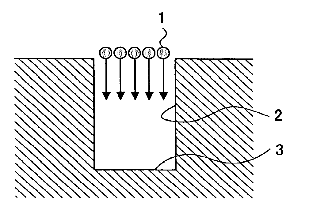
[0107]In order to deposit particles substantially on the bottom part in a groove structure having a high aspect ratio, such as the structure shown in FIG. 3, particles 1 having the same moving direction may be led to a bottom part 3 of a groove structure 2 having a high aspect ratio. In this case, it is necessary to form a particle beam wherein directions of particles are arranged in advance so as to have high directivities; and minimize disturbance, namely diffusion, of the particle direction due to a collision of gas molecules.

[0108]The groove structure having a high aspect ratio is assumed with a depth / width that is more than 1 / 1; that is, the depth is larger than the width, and the width is less than approximately 2 μm calculated under assumption that a particle size is approximately 20 nm.

[0109]More specifically, a deposition apparatus such as shown in FIG. 4 may be used. The deposition apparatus 4 includes a particle generation part 11, a particle charging part 12 for charging...

first example of first embodiment

[0124]Next, a first example of the first embodiment of a deposition method is explained. In addition, a deposition apparatus of fine particles, and a forming method and a forming apparatus of carbon nanotubes, are explained.

[0125]More specifically, in the first example, a deposition apparatus and method whereby particles are deposited substantially on a bottom part of a groove structure having a high aspect ratio such as a via hole forming part of a semiconductor wiring, and a method for growing carbon nanotubes by using the deposited particles as catalysts, are described.

[0126]FIG. 7 is a schematic view showing a schematic structure of a particle deposition apparatus of the first example of the first embodiment of the present invention. Nickel (Ni), Iron (Fe), Cobalt (Co), or the like is suitable as a catalyst particle. In this example, the Ni particle is used as the catalyst particle.

[0127]In this example, the particles are generated by using laser ablation. A Ni substrate 400 is ...

second example of first embodiment

[0140]Next, a second example of the first embodiment is explained. FIG. 11 is a schematic view showing a fine particle beam irradiation part of a particle deposition apparatus of the second example of the first embodiment.

[0141]In this example, the Ni particles are converged at the vacuum room 408 keeping a pressure of 102 Pa, for example, by using an aerodynamic lens 421. The aerodynamic lens 421 includes a plurality of circular plates 421a having holes. The circular plates 421a forming a lens are provided in a flow of gas. The particle beam is converged by using inertia of the particles when the flow repeats contraction and expansion. The proper diameter of the holes of the circular plates depends on the particle size, gas flow rate, and a pressure. In order to converge particles having a diameter of 5 nm under conditions of the above mentioned amount of flow and pressure, it is necessary to provide circular plates having holes whose diameter is approximately 12 mm. By arranging c...


PUM

PropertyMeasurementUnit
particle diametersaaaaaaaaaa
diameteraaaaaaaaaa

Abstract

A deposition method of fine particles, includes the steps of irradiating a fine particle beam formed by size-classified fine particles to an irradiated subject under a vacuum state, and depositing the fine particles on a bottom part of a groove structure formed at the irradiated subject.

Description

CROSS-REFERENCE TO RELATED APPLICATIONS[0001]This application is a division of U.S. application Ser. No. 10 / 874,392, filed on Jun. 24, 2004 which is based upon and claims the benefit of priority from the prior Japanese Priority Patent Application No. 2003-187331 filed on Jun. 30, 2003, and Japanese Priority Patent Application No. 2003-298337 filed on Aug. 22, 2003, the entire contents of which are hereby incorporated by reference.BACKGROUND OF THE INVENTION[0002]1. Field of the Invention[0003]The present invention relates to a deposition method and a deposition apparatus of fine particles such as nano-particles having diameters less than about 30 to 90 nm, and a forming method and a forming apparatus of carbon nanotubes by using the fine particles as catalysts.[0004]Furthermore, the present invention relates to semiconductor devices having a channel or wires for which carbon nanotubes are used and manufacturing methods of the same, and more particularly, to a semiconductor device ha...

Claims


Application Information

Patent Timeline
Patent Type & Authority Applications(United States)
IPC IPC(8): H01L23/48C23C14/56B05D3/06H01L21/768
CPCB82Y10/00B82Y30/00H01L2924/0002B82Y40/00C01B31/0233C01B2202/36C23C14/221C23C14/228C23C16/04C23C16/26H01L21/76867H01L21/76876H01L21/76879H01L23/53276H01L29/0673H01L29/0676H01L29/775H01L51/0048H01L51/0558H01L2221/1094H01L21/768H01L2924/00C01B32/16C01B32/162Y10S977/843H10K85/221H10K10/484H10K71/10C23C16/463C23C16/48
Inventor AWANO, YUJISHIMIZU, NORIYOSHISATO, SHINTARO
Owner FUJITSU LTD
Why Eureka
Try Eureka