
Method of growing GaN using CVD and HVPE

a technology of gan and gan, which is applied in the field of growing gan, can solve the problems of pollution, complex growing procedure, and thin gan obtained, and achieve the effects of improving the quality of gan

Inactive Publication Date: 2010-09-30
NAT SUN YAT SEN UNIV +1
View PDF2 Cites 1 Cited by
  • Summary
  • Abstract
  • Description
  • Claims
  • Application Information

AI Technical Summary

Benefits of technology

[0006]Another purpose of the present invention is to effectively mend a problem of spreading lithium element into gaps in GaN while using a LiAlO2 substrate.

Problems solved by technology

However, the growing procedure is complex and the GaN obtained is too thin.
If GaN is grown directly under HVPE by using a LiAlO2 substrate under a high temperature, a possible problem is that the lithium element in the substrate may be spread on a surface of the substrate before GaN nucleus sites are formed and thus a pollution may occur.
Consequently, the GaN obtained through the prior art may have HCl accumulated and lithium element spread into GaN structure, not to mention that the GaN obtained is too thin.
Hence, the prior art does not fulfill all users' requests on actual use.

Method used


Image

  • Method of growing GaN using CVD and HVPE
  • Method of growing GaN using CVD and HVPE
  • Method of growing GaN using CVD and HVPE

Examples


Embodiment Construction

[0013]The following description of the preferred embodiment is provided to understand the features and the structures of the present invention.

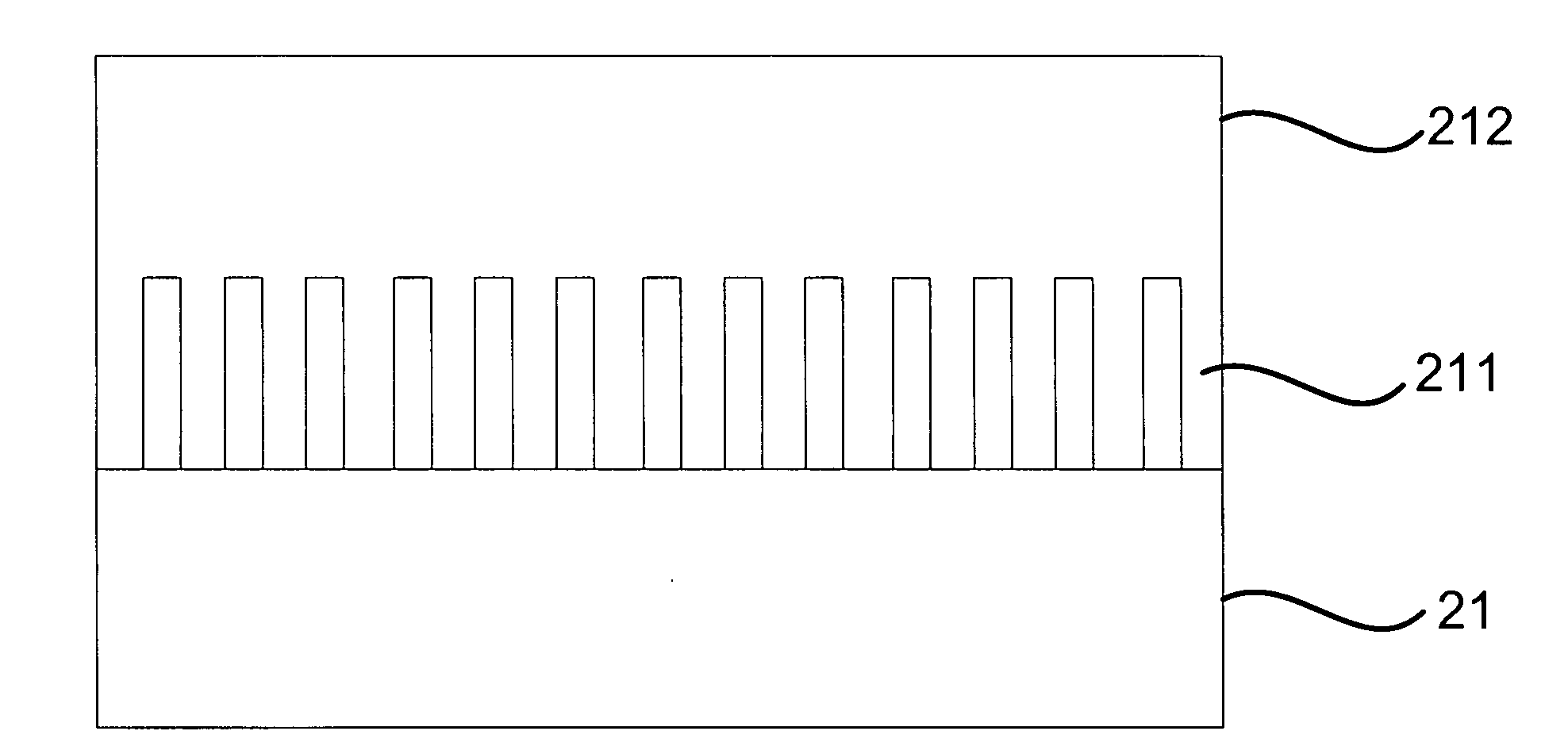
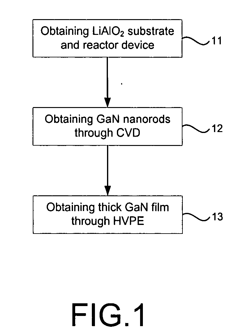
[0014]Please refer to FIG. 1 to FIG. 4, which are a flow view showing a preferred embodiment; a view showing a LiAlO2 substrate; a view showing a GaN nanorods; and a view showing a thick GaN film according to the present invention. As shown in the figures, the present invention is a method of growing GaN using CVD and HVPE, comprising the following steps:

[0015](a) Obtaining a LiAlO2 substrate and a reactor device 11: As shown in FIG. 2, a LiAlO2 substrate 21 and a reactor device (not shown in the figures) are obtained. The substrate made of LiAlO2 can be further a substrate made of sapphire (Al2O3), lithium gallium oxide (LiGaO2), lithium silicon oxide (Li2SiO3), lithium germanium oxide (LiGeO3), sodium aluminum oxide (NaAlO2), sodium germanium oxide (Na2GeO3), sodium silicon oxide (Na2SiO3), lithium phosphor oxide (Li3PO4), lithium arsenic o...


PUM


Abstract

A thick gallium nitride (GaN) film is formed on a LiAlO2 substrate through two stages. First, GaN nanorods are formed on the LiAlO2 substrate through chemical vapor deposition (CVD). Then the thick GaN film is formed through hydride vapor phase epitaxy (HVPE) by using the GaN nanorods as nucleus sites. In this way, a quantum confined stark effect (QCSE) becomes small and a problem of spreading lithium element into gaps in GaN on using the LiAlO2 substrate is mended.

Description

FIELD OF THE INVENTION[0001]The present invention relates to growing GaN; more particularly, relates to growing a thick GaN film on a GaN nucleus sites through a chemical vapor deposition (CVD) and a hydride vapor phase epitaxy (HVPE).DESCRIPTION OF THE RELATED ART[0002]An environment for growing GaN through CVD and HVPE usually uses a lot of ammonia (NH3) gas and hydrogen chloride (HCL) gas. And the HCl gas usually etches more surface than the NH3 gas.[0003]However, the growing procedure is complex and the GaN obtained is too thin. If GaN is grown directly under HVPE by using a LiAlO2 substrate under a high temperature, a possible problem is that the lithium element in the substrate may be spread on a surface of the substrate before GaN nucleus sites are formed and thus a pollution may occur.[0004]Consequently, the GaN obtained through the prior art may have HCl accumulated and lithium element spread into GaN structure, not to mention that the GaN obtained is too thin. Hence, the p...

Claims


Application Information

Patent Timeline
Patent Type & Authority Applications(United States)
IPC IPC(8): H01L21/20
CPCH01L21/0242H01L21/02458H01L21/0262H01L21/0254H01L21/02513
Inventor CHOU, MITCH M. C.HSU, WEN-CHING
Owner NAT SUN YAT SEN UNIV
Learn More