MFMS-FET, Ferroelectric Memory Device, And Methods Of Manufacturing The Same

a technology of ferroelectric memory and metal ferroelectric layer, which is applied in the direction of semiconductor devices, digital storage, instruments, etc., can solve the problems of deterioration of the polarization characteristics of the ferroelectric layer b>5/b>, short data retention time of the ferroelectric memory, and polarization characteristics of the ferroelectric layer

Inactive Publication Date: 2010-10-07
UNIVERSITY OF SEOUL
View PDF0 Cites 5 Cited by
  • Summary
  • Abstract
  • Description
  • Claims
  • Application Information

AI Technical Summary

Benefits of technology

[0011]Accordingly, the present invention has been made in an effort to solve the above-described problems, and an object of the present invention is to provide a field-effect transistor (FET), a ferroelectric memory device, which have a simple structure and excellent data retention characteristics, and methods of manufacturing the same.Technical Solution

Problems solved by technology

However, the ferroelectric memory having the above-described structure has the following problems.
As a result, there occurs a problem that the polarization characteristics of the ferroelectric layer 5 are deteriorated, that is, the data retention time of the ferroelectric memory becomes very short.
However, the MFIS type ferroelectric memory has some problems in that, since the buffer layer 20 formed between the ferroelectric layer 5 and the substrate 1 acts as a capacitor, the polarization characteristics of the ferroelectric layer 5 are deteriorated due to a depolarization field caused by the buffer layer 20, thus deteriorating the data retention characteristics.
As a result, the data retention time cannot exceed 30 days even in case of an excellent product manufactured in a laboratory.

Method used


Image

  • MFMS-FET, Ferroelectric Memory Device, And Methods Of Manufacturing The Same
  • MFMS-FET, Ferroelectric Memory Device, And Methods Of Manufacturing The Same
  • MFMS-FET, Ferroelectric Memory Device, And Methods Of Manufacturing The Same

Examples


first embodiment

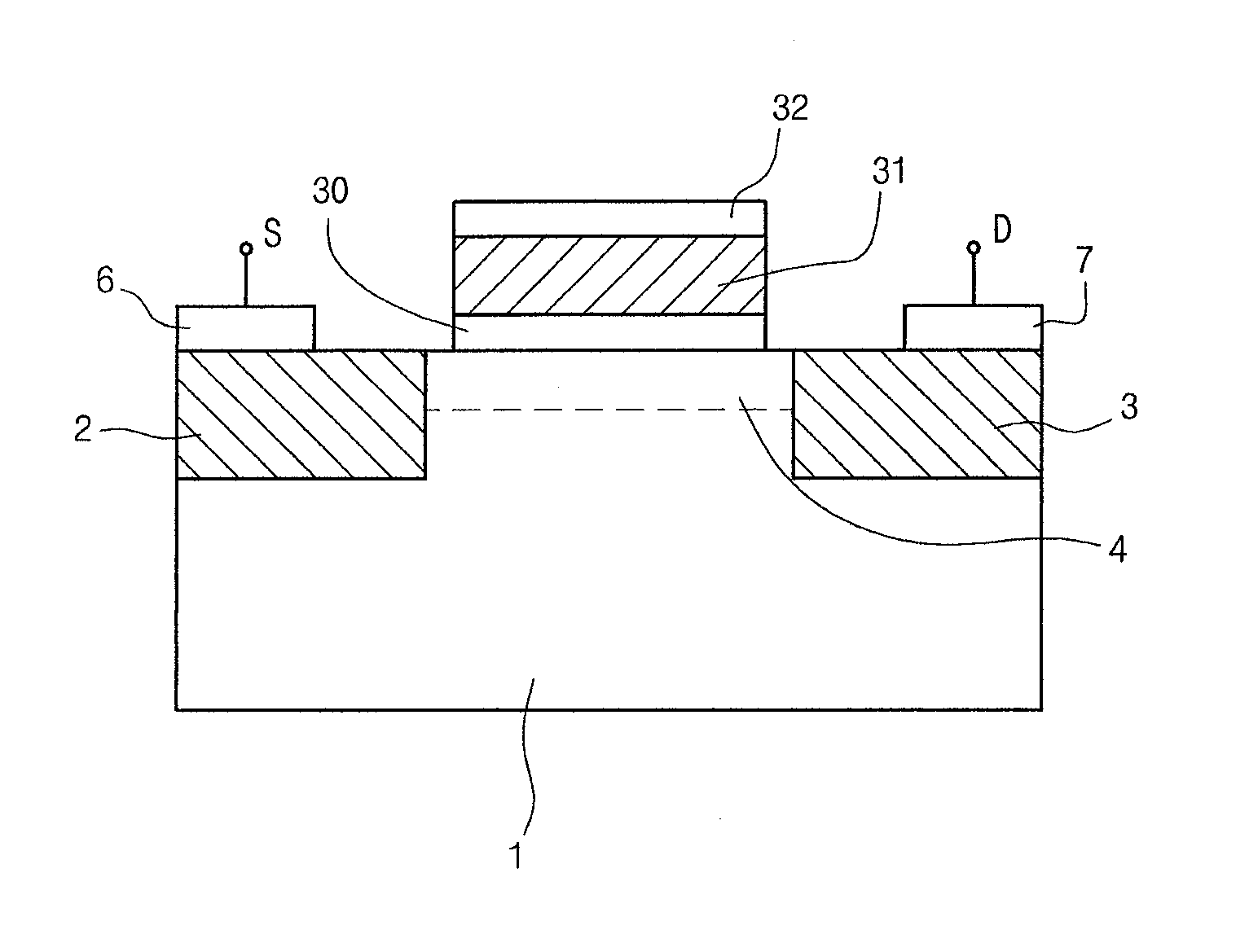
[0036]FIG. 4 is a cross-sectional view showing a structure of a field-effect transistor or a ferroelectric memory device in accordance with the present invention.

[0037]The ferroelectric memory device in accordance with the present invention has a metal-ferroelectric-metal-substrate (MFMS) structure, differently from a conventional metal-ferroelectric-semiconductor (MFS) structure and a conventional metal-ferroelectric-insulator-semiconductor (MFIS) structure.

[0038]As shown in FIG. 4, source and drain regions 2 and 3 are formed in predetermined areas of a silicon substrate 1, and a buffer layer 30 is formed of a conductive material on a channel region 4 between the source and drain regions 2 and 3.

[0039]In this case, the buffer layer 30 may comprise at least one selected from the group consisting of conductive metals such as gold (Au), silver (Ag), aluminum (Al), platinum (Pt), etc., conductive metal oxides such as RuO2, RuO2 / TiN, SrRuO3, YBCO, Pt / TiO2, Pt / IrOx, IrOx, TiN, ITO, SrTiO...

second embodiment

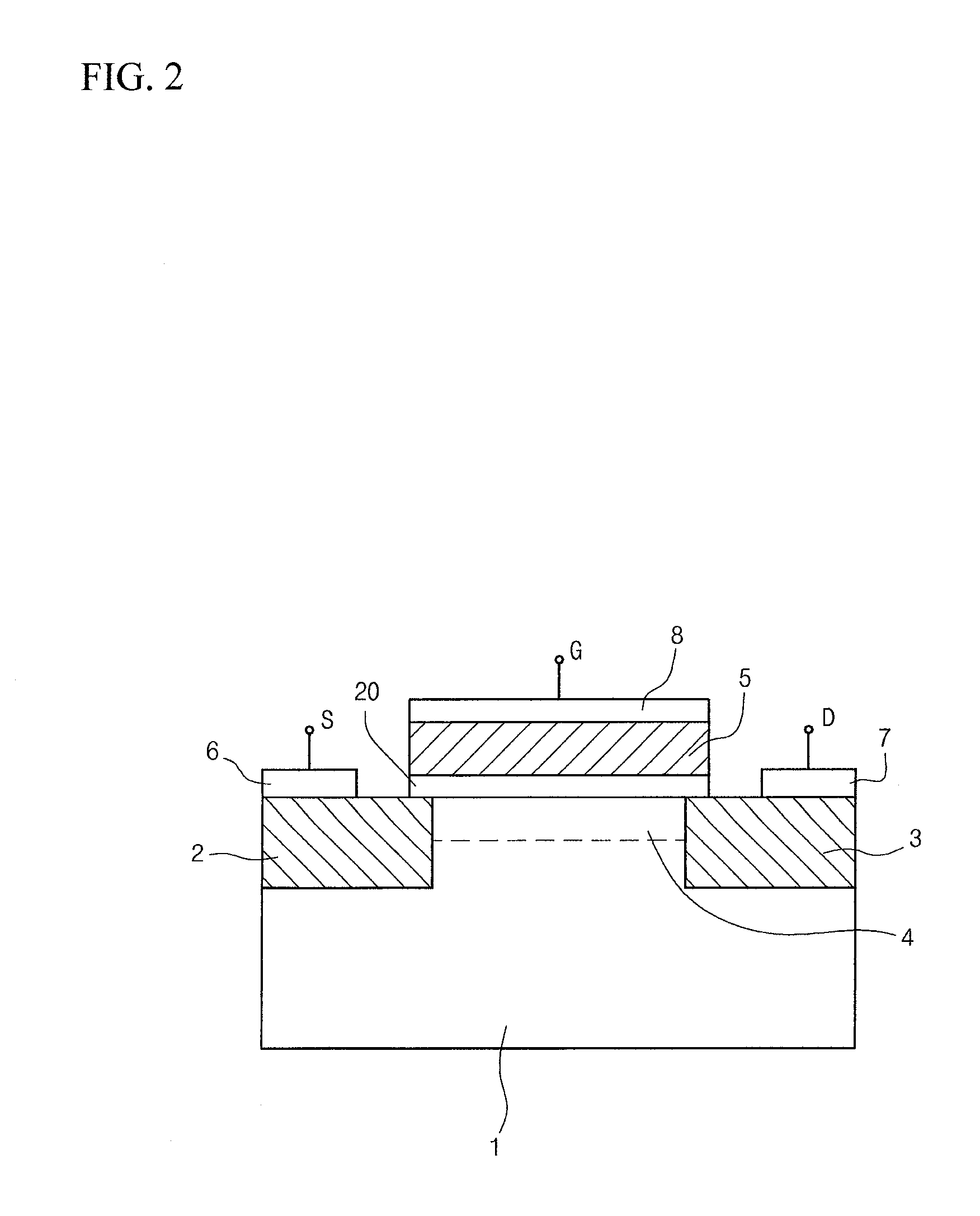
[0056]FIG. 6 is a cross-sectional view showing a structure of a field-effect transistor or a ferroelectric memory device in accordance with the present invention.

[0057]In the structure of FIG. 6, like the first embodiment of FIG. 4, source and drain regions 2 and 3 are formed on a silicon substrate 1, and a buffer layer 30 is formed of a conductive material on a channel region 4 between the source and drain regions 2 and 3.

[0058]In the present embodiment, an insulating layer 60 surrounding both sides of the buffer layer 30 is formed. The insulating layer 50 is formed of an insulating material such as LaZrO3, ZrO2, SiO2, etc. The insulating layer 60 prevents a current path from being formed between the buffer layer 30, formed of a conductive material, and the source and drain regions 2 and 3.

[0059]A ferroelectric layer 31 is formed on the buffer layer 30, and a gate electrode 32 is coated on the entire surface of the ferroelectric layer 31. And, since the other elements are substanti...

third embodiment

[0060]FIG. 7 is a cross-sectional view showing a structure of a field-effect transistor or a ferroelectric memory device in accordance with the present invention.

[0061]In FIG. 7, when a ferroelectric layer 31 is formed on a buffer layer 30, the ferroelectric layer 31 is coated on the entire surface of the buffer layer 30 so that the buffer layer 30 and source and drain regions 2 and 3 are shielded by the ferroelectric layer 31. And, since the other elements are substantially the same as those in the configuration of FIG. 6, the same elements as those of FIG. 6 are denoted by the same reference numerals, and their detailed descriptions will be omitted.

[0062]Meanwhile, FIG. 8 shows a process of manufacturing a field-effect transistor or a ferroelectric memory device in accordance with the present invention, which particularly shows a process of manufacturing the structure of FIG. 6.

[0063]First, a photoresist 81 is deposited on a substrate 1, and source and drain regions 2 and 3 are fo...


PUM


Abstract

Disclosed herein are a metal-ferroelectric-metal-substrate (MFMS) field-effect transistor (FET), an MFMS-ferroelectric memory device, and method of manufacturing the same. The MFMS-FET and the ferroelectric memory device in accordance with the present invention include: a substrate including source and drain regions, and a channel region formed therebetween; a buffer layer formed on the top of the channel region of the substrate; a ferroelectric layer formed on the buffer layer; and a gate electrode formed on the ferroelectric layer, wherein the buffer layer is formed of a conductive material.

Description

TECHNICAL FIELD[0001]The present invention relates to a metal-ferroelectric-metal-substrate (MFMS) field-effect transistor (FET) and a ferroelectric memory device having a simple structure and excellent data retention characteristics.BACKGROUND ART[0002]At present, extensive research aimed at realizing a transistor or a memory device using a ferroelectric material has continued to progress. FIG. 1 is a cross-sectional view showing a typical structure of a metal-ferroelectric-semiconductor (MFS) ferroelectric memory device using a ferroelectric material.[0003]As shown in FIG. 1, source and drain regions 2 and 3 are formed in predetermined areas of a silicon substrate 1, and a ferroelectric layer 5 is formed on a channel region 4 between the source and drain regions 2 and 3. In this case, the ferroelectric layer 5 comprises an inorganic material having ferroelectric characteristics such as PbZrxTi1-xO3 (PZT), SrBi2Ta2O9 (SBT), (Bi,La)4Ti3O12 (BLT), and the like. Moreover, a source ele...

Claims


Application Information

Patent Timeline
Patent Type & Authority Applications(United States)
IPC IPC(8): H01L27/105H01L21/8232H01L21/338
CPCH01L21/28291H01L29/47H01L29/78391H01L29/516H01L29/6684H01L29/512G11C11/22G11C11/223H01L29/40111H01L21/265H01L21/31051
Inventor PARK, BYUNG-EUN
Owner UNIVERSITY OF SEOUL
Why Eureka
Try Eureka