On-chip leakage current modeling and measurement circuit

a leakage current and measurement circuit technology, applied in the field of design characterization methods and circuits, can solve the problems of inability to accurately measure leakage current, difficult to model leakage current across a die, and inability to distinguish between leakage of different device types

Active Publication Date: 2010-10-07
GLOBALFOUNDRIES US INC
View PDF6 Cites 21 Cited by
  • Summary
  • Abstract
  • Description
  • Claims
  • Application Information

AI Technical Summary

Problems solved by technology

In very large-scale integrated circuits (VLSI) such as semiconductor memories and microprocessors, accurate leakage current measurement is typically not possible, since measurement of true leakage current requires that all of the devices under measurement be in an “off” state, which generally cannot be commanded at the same time across an entire integrated circuit die.
Leakage current across a die is difficult to model, and any model will deviate substantially from actual leakage current, as the combination of local variation with variation of the design values combines significantly, particularly in present-day low voltage technologies, in which the power supply voltages are decreasing to below one volt.
Present leakage current monitoring circuits typically measure a leakage of one or more devices to estimate total leakage of a device, but are not typically statistically representative of an integrated circuit design as a whole, with the exception of actual total device leakage current measurements, which can only provide measurement of the current consumed by an integrated circuit while the internal circuits are in a suspended state.
Even in a suspended state, all devices are typically not in their “off” state, as noted above, and there is no ability to distinguish between leakage of different device types.
Other test and measurement circuits may be provided to make leakage current measurements and / or model device current leakage, but also fail to provide a measure of true off-state leakage and fail to provide a model sufficiently accurate to the describe the actual integrated circuit.

Method used


Image

  • On-chip leakage current modeling and measurement circuit
  • On-chip leakage current modeling and measurement circuit
  • On-chip leakage current modeling and measurement circuit

Examples


Embodiment Construction

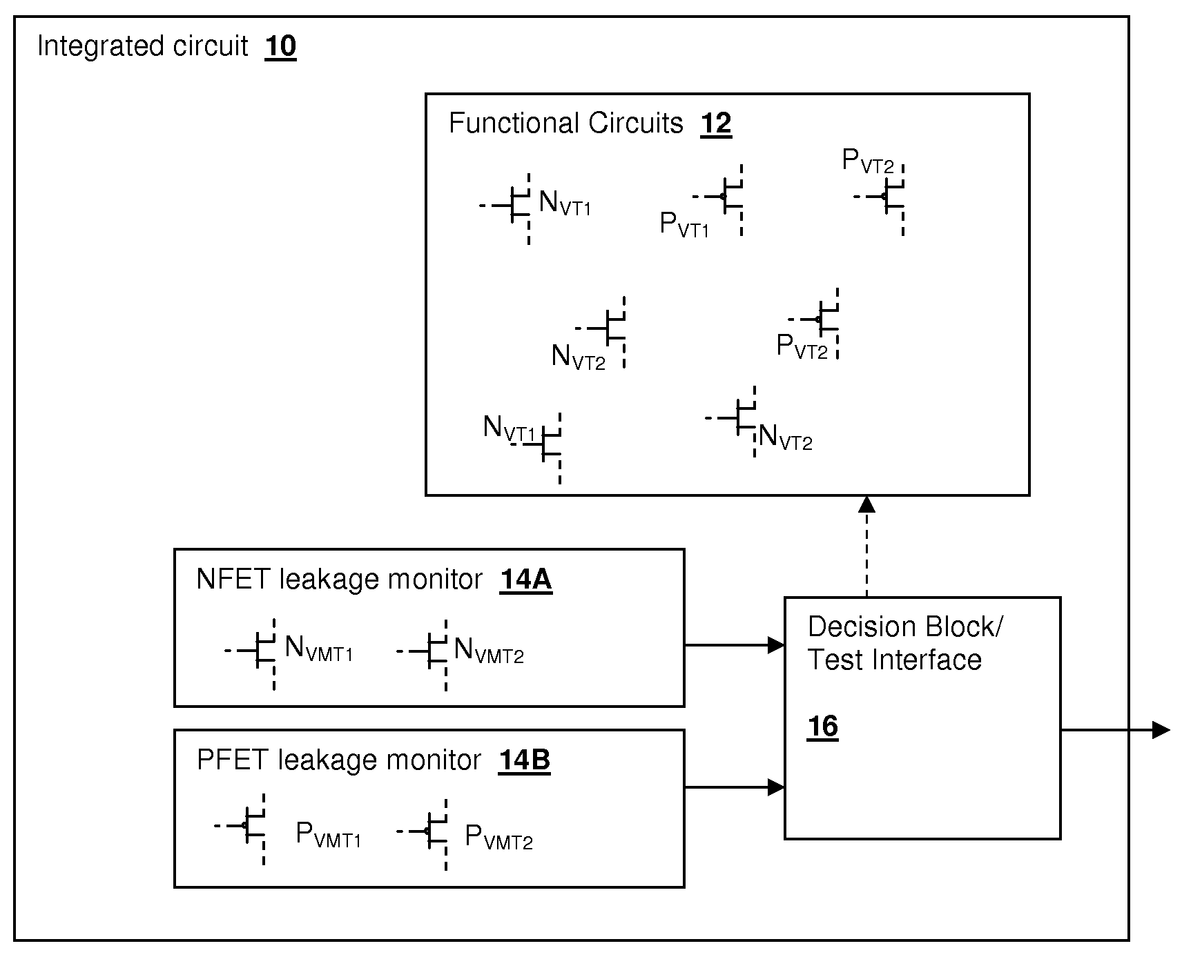
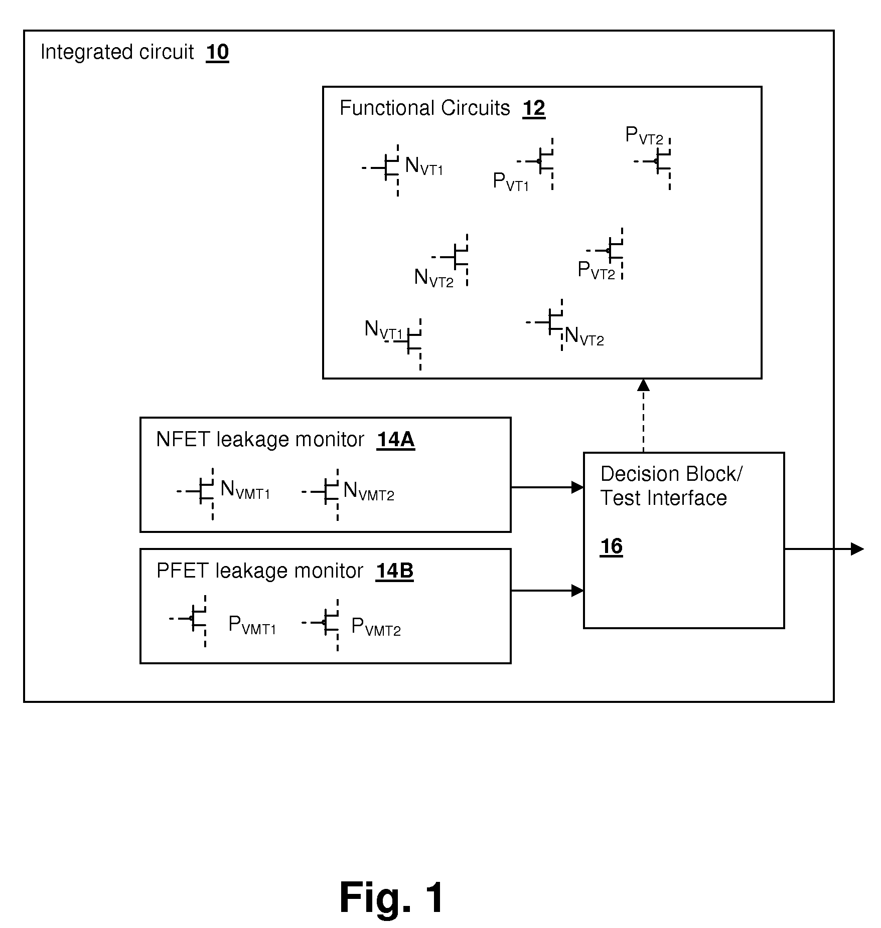
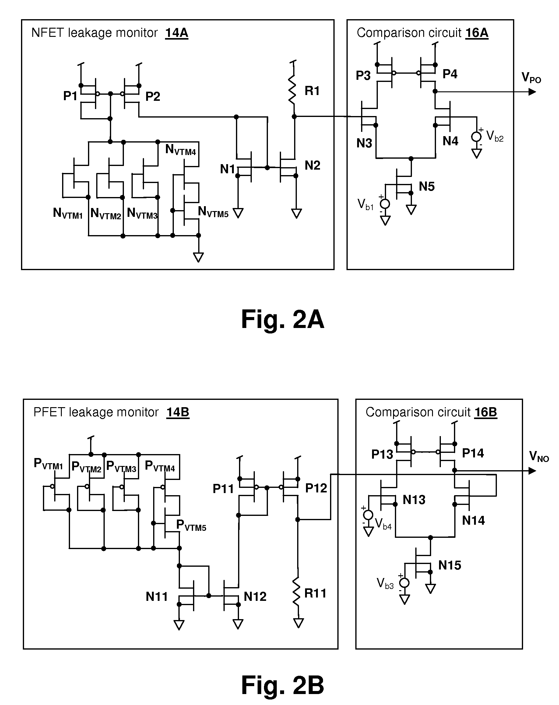
[0019]The present invention relates to a leakage current monitor circuit integrated on a die, methodologies for determining true off-state current leakage of a separate functional digital circuit integrated on the die, and systems using are such a leakage current monitor circuit to monitor and / or control the operating conditions of the digital circuit, as well as to evaluate a design of the integrated circuit. The present invention also encompasses methodologies for designing such a monitor circuit. The leakage current monitor circuit has both N-type and P-type transistors sized to represent the aggregated area of all of the N-type and P-type transistors in the digital circuit, and may include multiple N-type and P-type transistors sized according to an aggregated area of classes of the N-type and P-type transistors having differing threshold voltages.

[0020]Referring now to FIG. 1, an integrated circuit 10 in accordance with an embodiment of the present invention is shown. Functiona...


PUM


Abstract

A leakage current monitor circuit provides an accurate statistically representative analog of true off-state leakage current in a digital circuit integrated on a die. At least one N-type transistor and at least one P-type transistor separate from the digital circuit are sized to represent the total area of the corresponding type transistors in the digital circuit. The gates of the N-type transistor and P-type transistors are set to voltages according to the corresponding off-state logic levels of the digital circuit. The N-type and P-type transistors form a portion of corresponding current mirror circuits, which can provide outputs to a leakage current monitor and / or a control circuit such as a comparator that determines when leakage current for the N-type or P-type devices has exceeded a threshold. The output of the measurement / control circuit can be used to determine a temperature of and / or control operation of the digital circuit or the system environment of the integrated circuit.

Description

BACKGROUND OF THE INVENTION[0001]1. Field of the Invention[0002]The present invention is related to design characterization methods and circuits, and more particularly to integrated circuits having on-chip leakage current monitors, such as leakage current estimation or measurement circuits.[0003]2. Description of Related Art[0004]In very large-scale integrated circuits (VLSI) such as semiconductor memories and microprocessors, accurate leakage current measurement is typically not possible, since measurement of true leakage current requires that all of the devices under measurement be in an “off” state, which generally cannot be commanded at the same time across an entire integrated circuit die. Further, even if all leakage current paths have an “off” device (e.g., a CMOS circuit in a static state), both “off” devices and “on” devices vary in type and strength across the die. Leakage current across a die is difficult to model, and any model will deviate substantially from actual leak...

Claims


Application Information

Patent Timeline
Patent Type & Authority Applications(United States)
IPC IPC(8): G06F17/50G01R19/00
CPCG01R31/025G11C29/006G11C2029/5602G11C29/50G11C2029/5006G11C29/028G01R31/52
Inventor JOSHI, RAJIV V.KANJ, ROUWAIDA N.KUANG, JENTE B.NASSIF, SANI R.
Owner GLOBALFOUNDRIES US INC
Why Eureka
Try Eureka