

Effective gate length circuit modeling based on concurrent length and mobility analysis
a technology of gate applied in the field of effective gate length circuit modeling based on concurrent length and mobility analysis, can solve problems such as excessive standby power dissipation and reliability problems
- Summary
- Abstract
- Description
- Claims
- Application Information
AI Technical Summary
Benefits of technology
Problems solved by technology
Method used
Image

Examples
Embodiment Construction
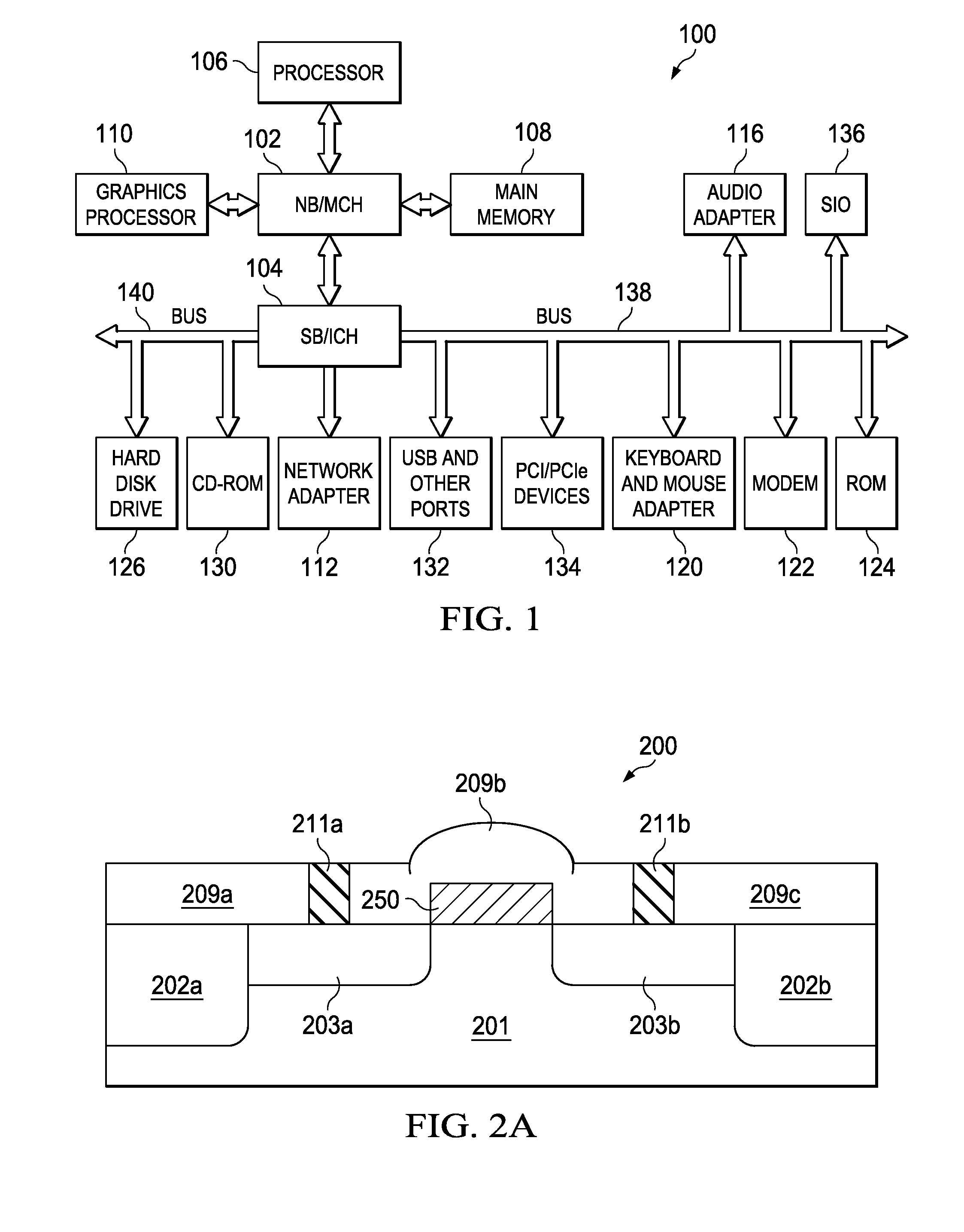
[0018]With reference now to the figures and in particular with reference to FIG. 1, a block diagram of a data processing system is shown in which aspects of an illustrative embodiment may be implemented. Data processing system 100 is an example of a computer, in which code or instructions implementing the processes of the present invention may be located. In the depicted example, data processing system 100 employs a hub architecture including a north bridge and memory controller hub (NB / MCH) 102 and a south bridge and input / output (I / O) controller hub (SB / ICH) 104. Processor 106, main memory 108, and graphics processor 110 connect to north bridge and memory controller hub 102. Graphics processor 110 may connect to the NB / MCH through an accelerated graphics port (AGP), for example.
[0019]In the depicted example, local area network (LAN) adapter 112 connects to south bridge and I / O controller hub 104 and audio adapter 116, keyboard and mouse adapter 120, modem 122, read only memory (RO...
PUM
 Abstract
Description
Claims
Application Information