Field effect transistor having graphene channel layer

a field effect transistor and graphene channel technology, applied in the field of field effect transistors, can solve the problems of large area integration, low on/off ratio, large integration and high-speed operation, and achieve the effect of increasing the on/off ratio of an operating curren

Active Publication Date: 2010-10-14
ELECTRONICS & TELECOMM RES INST
View PDF8 Cites 117 Cited by
  • Summary
  • Abstract
  • Description
  • Claims
  • Application Information

AI Technical Summary

Benefits of technology

[0010]The present invention provides a field effect transistor having a graphene channel layer, that is, a field ef

Problems solved by technology

Large area integration is difficult in the case of using carbon nanotubes in the formation of transistors.
Such a low on/off ratio works against large integration and high-speed operation of a field effect transistor.
However, according to the suggested methods descr

Method used


Image

  • Field effect transistor having graphene channel layer
  • Field effect transistor having graphene channel layer
  • Field effect transistor having graphene channel layer

Examples


Embodiment Construction

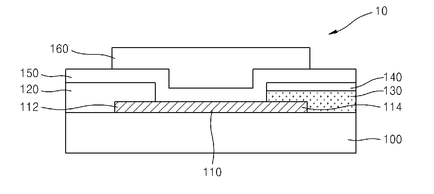
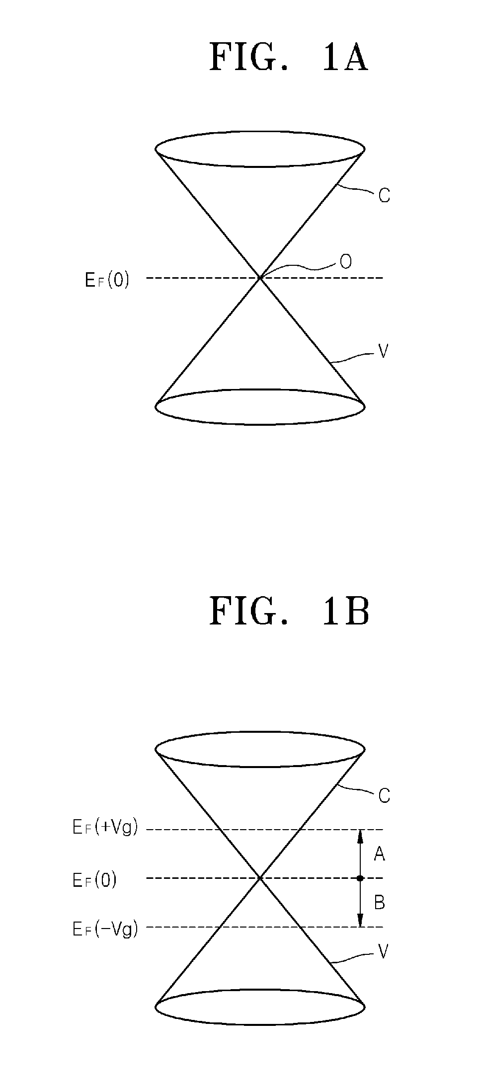
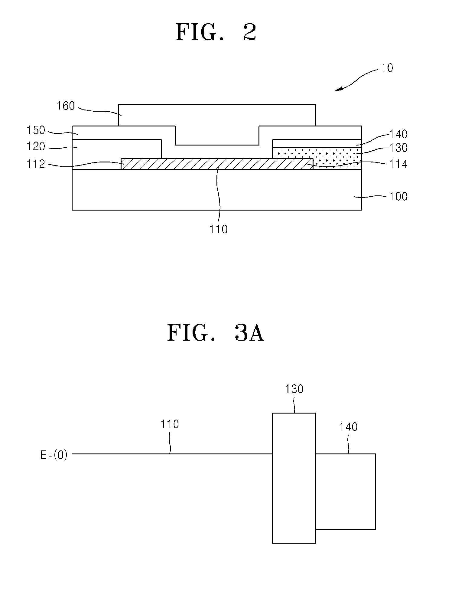
[0038]Reference will now be made in detail to exemplary embodiments, examples of which are illustrated in the accompanying drawings. However, exemplary embodiments are not limited to the embodiments illustrated hereinafter, and the embodiments herein are rather introduced to provide easy and complete understanding of the scope and spirit of exemplary embodiments. In the drawings, the thicknesses of layers and regions are exaggerated for clarity.

[0039]It will be understood that when an element, such as a layer, a region, or a substrate, is referred to as being “on,”“connected to” or “coupled to” another element, it may be directly on, connected or coupled to the other element or intervening elements may be present. In contrast, when an element is referred to as being “directly on,”“directly connected to” or “directly coupled to” another element or layer, there are no intervening elements or layers present. Like reference numerals refer to like elements throughout. As used herein, the...


PUM


Abstract

Provided is a field effect transistor including a graphene channel layer, and capable of increasing an on/off ratio of an operating current by using the graphene of the graphene channel layer. The field effect transistor includes: a substrate; the graphene channel layer which is disposed on a portion of the substrate and includes graphene; a first electrode disposed on a first region of the graphene channel layer and a portion of the substrate; an interlayer disposed on a second region of the graphene channel layer, which is apart from the first region, and a portion of the substrate; a second electrode disposed on the interlayer; a gate insulation layer disposed on a portion of the graphene channel layer, the first electrode, and the second electrode; and a gate electrode disposed on a portion of the gate insulation layer.

Description

CROSS-REFERENCE TO RELATED PATENT APPLICATION[0001]This application claims the benefit of Korean Patent Application No. 10-2009-0030516, filed on Apr. 8, 2009, in the Korean Intellectual Property Office, the disclosure of which is incorporated herein in its entirety by reference.BACKGROUND OF THE INVENTION[0002]1. Field of the Invention[0003]The present invention relates to a field effect transistor, and more particularly, to a field effect transistor using graphene in a channel layer.[0004]2. Description of the Related Art[0005]Kostya Novoselov and Andre Geim were first to discover how to fabricate graphene, which consists of two dimensional carbon atoms in a hexagonal structure, by mechanically exfoliating graphite, and have reported field effect characteristics exhibited by the graphene, numerous attempts of fabricating highly efficient transistors with high operating speed using graphene are being made.[0006]Graphene is a carbon nanostructure that has a two-dimensional shape, hi...

Claims


Application Information

Patent Timeline
IPC IPC(8): H01L29/08
CPCH01L29/0673H01L29/0895H01L29/1606H01L29/78696H01L29/78684H01L51/0541H01L29/778H10K10/464H01L29/42312H01L29/4232
Inventor CHAE, BYUNG-GYUKIM, HYUN TAK
Owner ELECTRONICS & TELECOMM RES INST
Why Eureka
Try Eureka