Substrate and semiconductor device

Active Publication Date: 2010-10-14
RENESAS ELECTRONICS CORP
View PDF3 Cites 15 Cited by
  • Summary
  • Abstract
  • Description
  • Claims
  • Application Information

AI Technical Summary

Benefits of technology

[0022]According to the present invention, on the substrate which includes the pads and the insulating film having openings which at least partially expose the pads therein, which are formed over one surface of the b

Problems solved by technology

The conventional configurations have, however, been incapable of effectively prevent the separation between the pad and the base, u

Method used


Image

  • Substrate and semiconductor device
  • Substrate and semiconductor device
  • Substrate and semiconductor device

Examples


Example

[0034]The invention will now be described herein with reference to illustrative embodiments. Those skilled in the art will recognize that many alternative embodiments can be accomplished using the teachings of the present invention and that the invention is not limited to the embodiments illustrated for explanatory purposes.

[0035]Embodiments of the present invention will be explained below, referring to the attached drawings. Note that whatever similar constituents in all drawings will be given similar reference numerals or symbols, and relevant explanations will not be repeated.

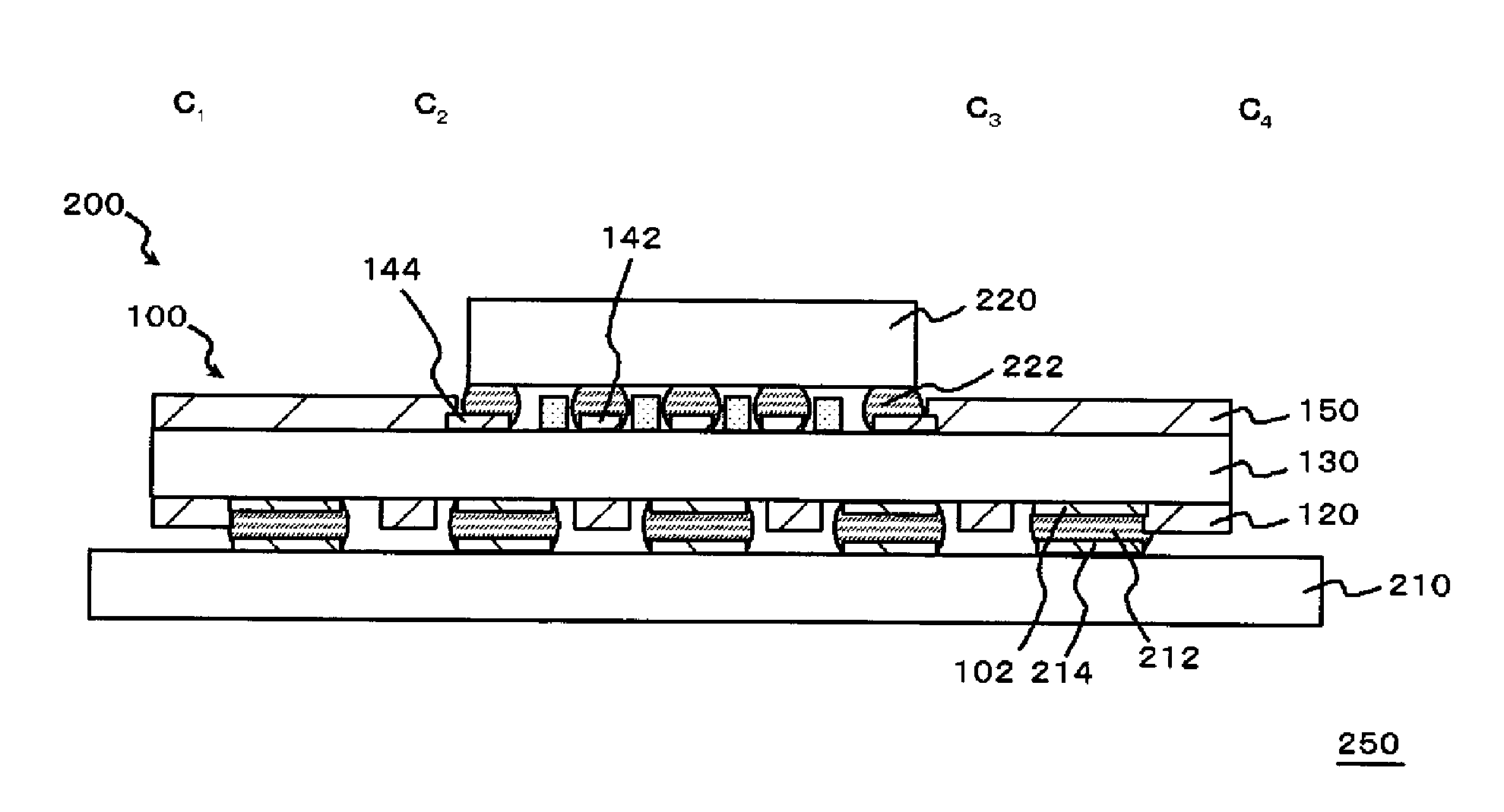
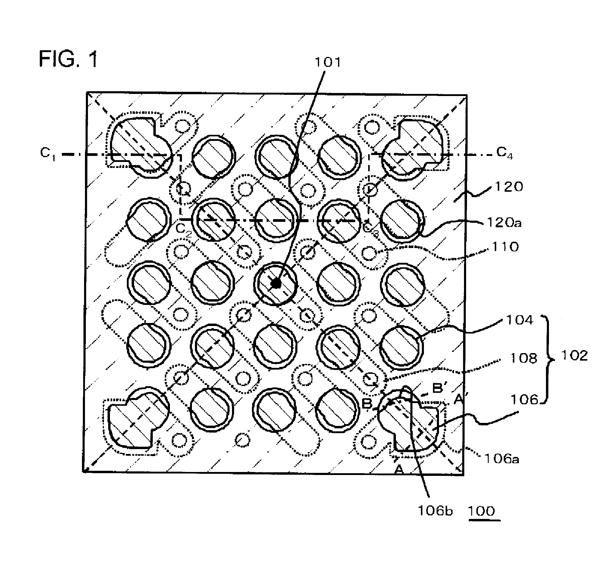
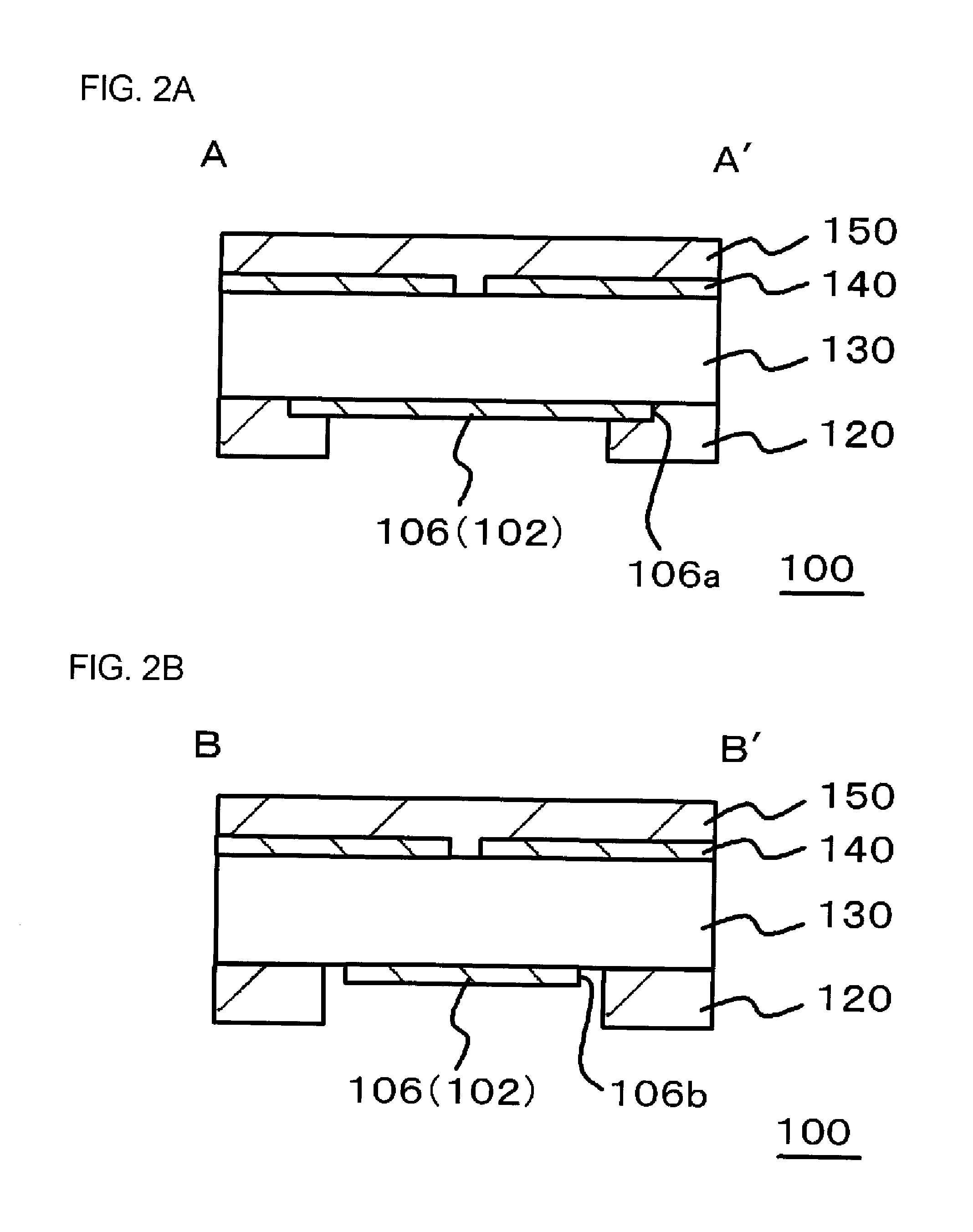
[0036]FIG. 1 is a plan view illustrating an exemplary configuration embodied on one surface of a substrate in one embodiment of the present invention. FIG. 2A is a sectional view taken along line A-A′ in FIG. 1, and FIG. 2B is a sectional view taken along line B-B′ in FIG. 1.

[0037]As illustrated in FIGS. 2A and 2B, a substrate 100 includes a base 130, an interconnect pattern 102 and a solder resist layer 120...


PUM


Abstract

A substrate has a plurality of pads formed over one surface of a base, and an insulating film which is formed thereon and has a plurality of openings formed therein so as to expose each of the pads, wherein the openings of the insulating film are formed so that, in each pad formed at the corner of the base, among the plurality of pads, a first peripheral portion which composes a portion of the pad more closer to the corner and more distant away from the center of the base is covered by the insulating film, and so that a second peripheral portion which composes a portion of the pad more closer to the center as compared with the first peripheral portion is exposed in the opening.

Description

[0001]This application is based on Japanese patent application No. 2009-095298, the content of which is incorporated hereinto by reference.BACKGROUND[0002]1. Technical Field[0003]The present invention relates to a substrate and a semiconductor device.[0004]2. Related Art[0005]A semiconductor element and an external electronic circuit substrate such as a mother board are connected generally as described below. First, the semiconductor element is mounted on an interposer such as printed substrate, and the product is then made up to a package in a form of LGA (land grid array) having flat electrode pads arranged on one surface of the interposer, BGA (ball grid array) further having solder balls disposed on the similar flat electrode pads, or the like. The package is then electrically connected to the external electronic circuit substrate such as the mother board, while placing a solder paste in between.[0006]The flat electrode pad herein is configured by a portion of an interconnect pa...

Claims


Application Information

Patent Timeline
IPC IPC(8): H01L23/538H05K1/18
CPCH01L23/49816H01L23/49838H05K1/111H05K3/3436H05K3/3452H01L2224/16237H05K2201/094H05K2201/0989H05K2201/099H05K2201/10674H05K2201/10734H05K2201/09381H01L2224/81385H01L2224/0558H01L2224/05573H01L2224/05568H01L2224/05147H01L2224/05644H01L2224/05655H01L2924/00014H01L24/05Y02P70/50H01L2224/05599
Inventor TAKEDA, HIROMITSU
Owner RENESAS ELECTRONICS CORP
Why Eureka
Try Eureka