Photonic crystal LED

Active Publication Date: 2010-10-28
LUMILEDS
View PDF8 Cites 6 Cited by
  • Summary
  • Abstract
  • Description
  • Claims
  • Application Information

AI Technical Summary

Benefits of technology

[0029]More particularly, the sub-electrodes may be associated with a respective photonic crystal. It is preferred to match the size and shape of the sub-electrodes to the size and shape of the respective photonic crystal. In this manner, easier and more predictable control of the far field emission may be provided. It shall be noted that some of the electrodes may be associated with a surface area of the LED that does not contain a photonic crystal, but that surface area may have been treated by other techniques like roughening to obtain a homogeneous emission pattern.
[0030]Hence, according to the above mentioned embodiment of the present invention, there is provided an LED, in which one of the electrodes is divided into sub-electrodes, wherein each sub-electrode is individually controllable by means of applying a voltage at each one of the sub-electrodes. An advantage with this embodiment is that the intensity distribution (brightness)of the light emitted from the LED may be controlled by selecting different voltages (also no voltage at all is a possible option) for different sub-electrodes.
[0031]Furthermore, heat transfer from the

Problems solved by technology

Many light emitting diodes (LEDs) suffer from poor extraction efficiency, i.e. the amount of light escaping from a light emitting diode (LED) compared to the light generated in the LED is small.
A common problem of LEDs is that total internal reflection of the light in the LED material causes the light to be trapped within the LED and, hence, it does not escape from the LED.
One cause of total internal reflection is that there is a large difference in index of refraction between the light emitting material and

Method used


Image

  • Photonic crystal LED
  • Photonic crystal LED
  • Photonic crystal LED

Examples


Embodiment Construction

[0044]In the following Figures, similar reference numerals have been used for similar parts or features throughout the description when applicable.

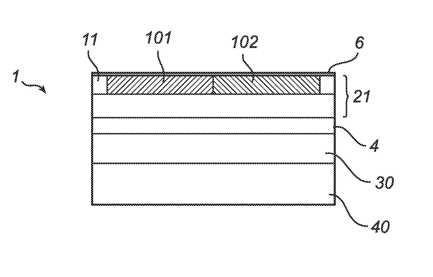
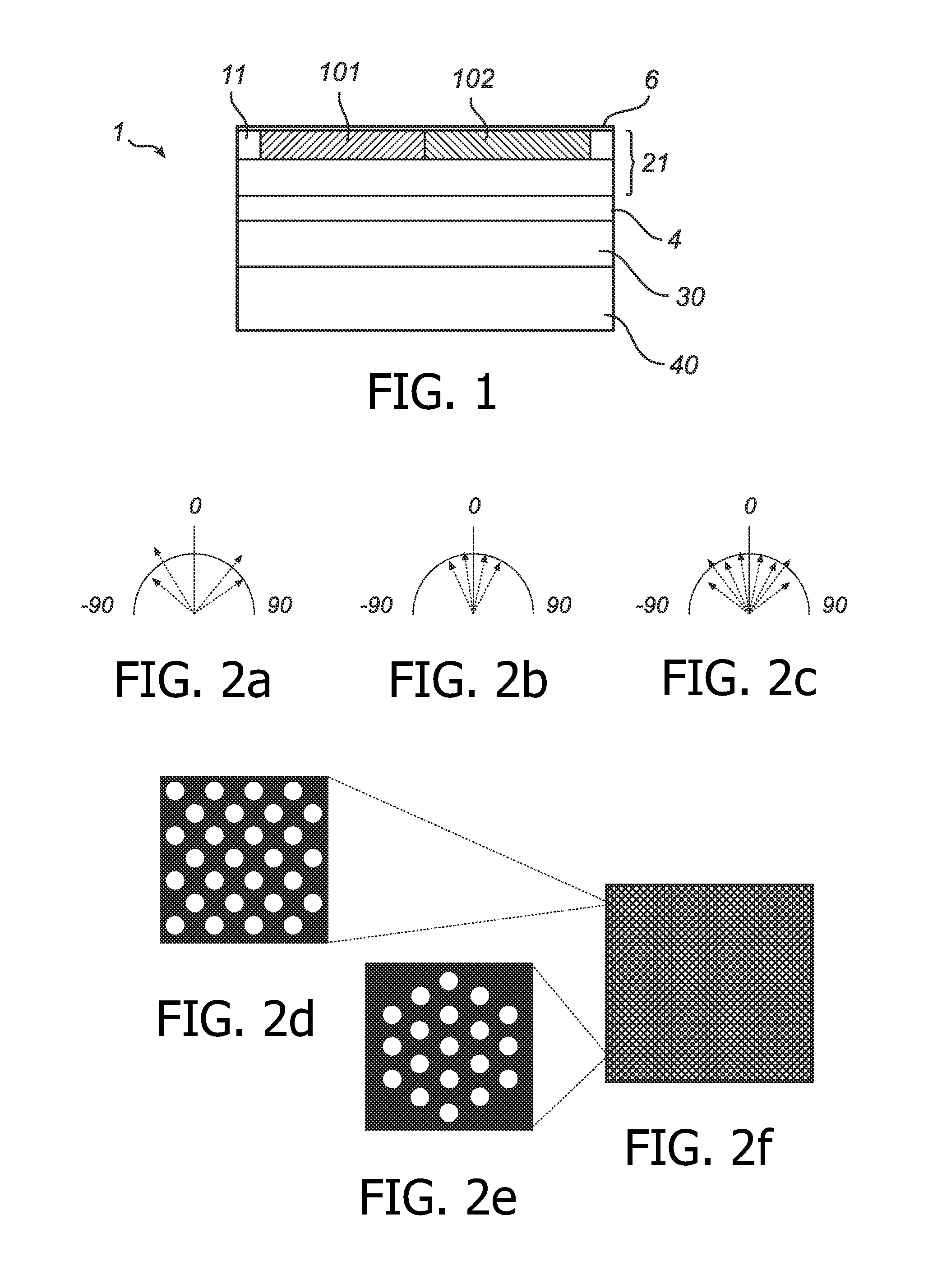
[0045]In FIG. 1, there is shown an exemplifying light emitting diode 1 (LED) according to an embodiment of the present invention. The LED 1 comprises a semiconductor stack of epitaxial layers 21, 30. In this particular example, the semiconductor stack has a total thickness of 400 nm and is manufactured from GaN. The stack comprises (from bottom to top according to FIG. 1) a first electrode 40, a P-type semiconductor layer 30 in connection with the first electrode 40, an active region 4, an N-type layer 21, a second electrode 11 (or electrode arrangement) in connection with the N-type layer 21 and a light emitting area (light emitting surface) 6. The photonic crystals 101, 102 are formed as holes in the N-type layer 21. The thickness of the photonic crystal layer 101, 102 may be increased such as to extend into the active region (quantum w...


PUM


Abstract

A semiconductor light emitting diode (1, LED), comprising a first and a second electrode (40, 11) for applying a voltage across an active region (4) for generation of light, a light emitting surface (6), and a plurality of photonic crystals (101, 102). Further, at least two photonic crystals (101, 102) of a first and a second type are adapted to extract light from the active region (4) and differ from each other with respect to at least one lattice parameter. Each of said at least two photonic crystals (101, 102) are associated with a respective far field pattern, wherein an arrangement of said plurality of photonic crystals (101, 102) is provided to arrange said at least two photonic crystals (101, 102). In this manner, a far field pattern is created by combining the respective far field patterns associated with each of said at least two photonic crystals (101, 102).

Description

FIELD OF THE INVENTION[0001]The present invention relates to a light emitting diode, comprising photonic crystals.BACKGROUND OF THE INVENTION[0002]In the modern society of today, the use of light emitting diodes emitting visible light is wide spread. Applications of light emitting diodes include light emitting signs, such as exit signs or emergency signs, lights for vehicles, such as breaking lights, backlight illumination for large scale video displays and illumination systems for furniture, such as shelves. However, the use of light emitting diodes for applications like projection sources or car headlamps is growing less rapidly, due to the fact that the emission angle of a generic light emitting diode is wide. For these applications, it is desired to use a light source having highly collimated light.[0003]Many light emitting diodes (LEDs) suffer from poor extraction efficiency, i.e. the amount of light escaping from a light emitting diode (LED) compared to the light generated in ...

Claims


Application Information

Patent Timeline
IPC IPC(8): H01L33/02H01L33/44H01L33/38H01L33/58
CPCH01L33/02H01L33/387H01L2933/0083H01L33/58H01L33/44
Inventor VERSCHUUREN, MARCUS ANTONIUSVAN SPRANG, HENDRIK ADRIANUS
Owner LUMILEDS
Why Eureka
Try Eureka