Semiconductor device and method for manufacturing metallic shielding plate

Active Publication Date: 2010-10-28
DAI NIPPON PRINTING CO LTD
View PDF10 Cites 11 Cited by
  • Summary
  • Abstract
  • Description
  • Claims
  • Application Information

AI Technical Summary

Benefits of technology

[0023]As outlined above, according to the present invention, since sharp burrs of a metallic shielding plate, formed at distal ends of other burrs in a manufacturing process for a semiconductor device, are kept out of contact with a semiconductor chip and a substrate, this characteristic prevents the semiconductor chip from being damaged by contact with the sharp burrs of the metallic shielding plate.
[0024]In addition, according to the present invention, worked permalloy PC materials are subjected to heat treatment at 650° C. to 850° C. under an inert gas atmosphere in

Problems solved by technology

During the manufacture of semiconductor devices, however, sharp burrs occur at the connections of each metallic shielding plate and if

Method used


Image

  • Semiconductor device and method for manufacturing metallic shielding plate
  • Semiconductor device and method for manufacturing metallic shielding plate
  • Semiconductor device and method for manufacturing metallic shielding plate

Examples


first embodiment

[0058]Hereunder, a first embodiment of the present invention will be described with reference made to the accompanying drawings. FIGS. 1 to 23 illustrate the first embodiment of the present invention.

(Configuration of a Metallic Shielding Sheet)

[0059]First, a metallic shielding sheet is outlined below in accordance with FIGS. 1 to 3(a) to 3(d).

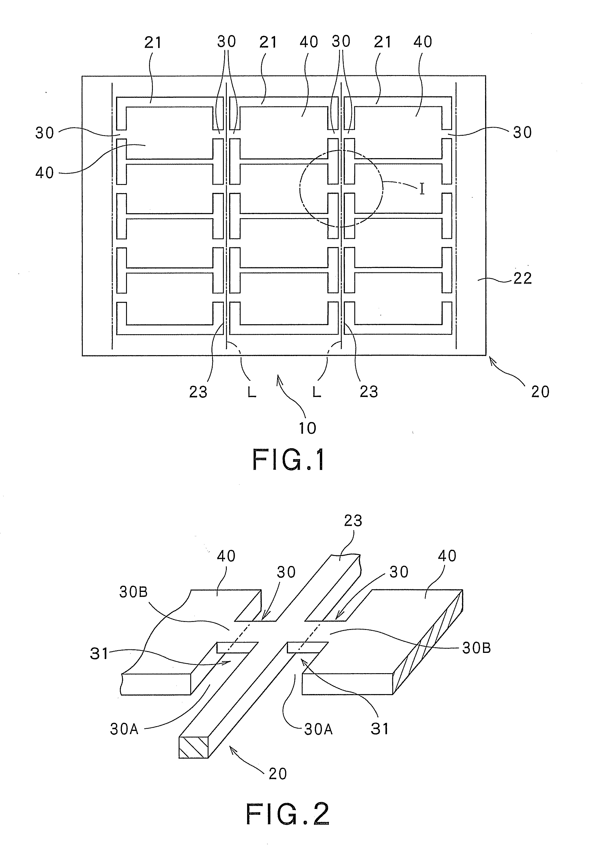
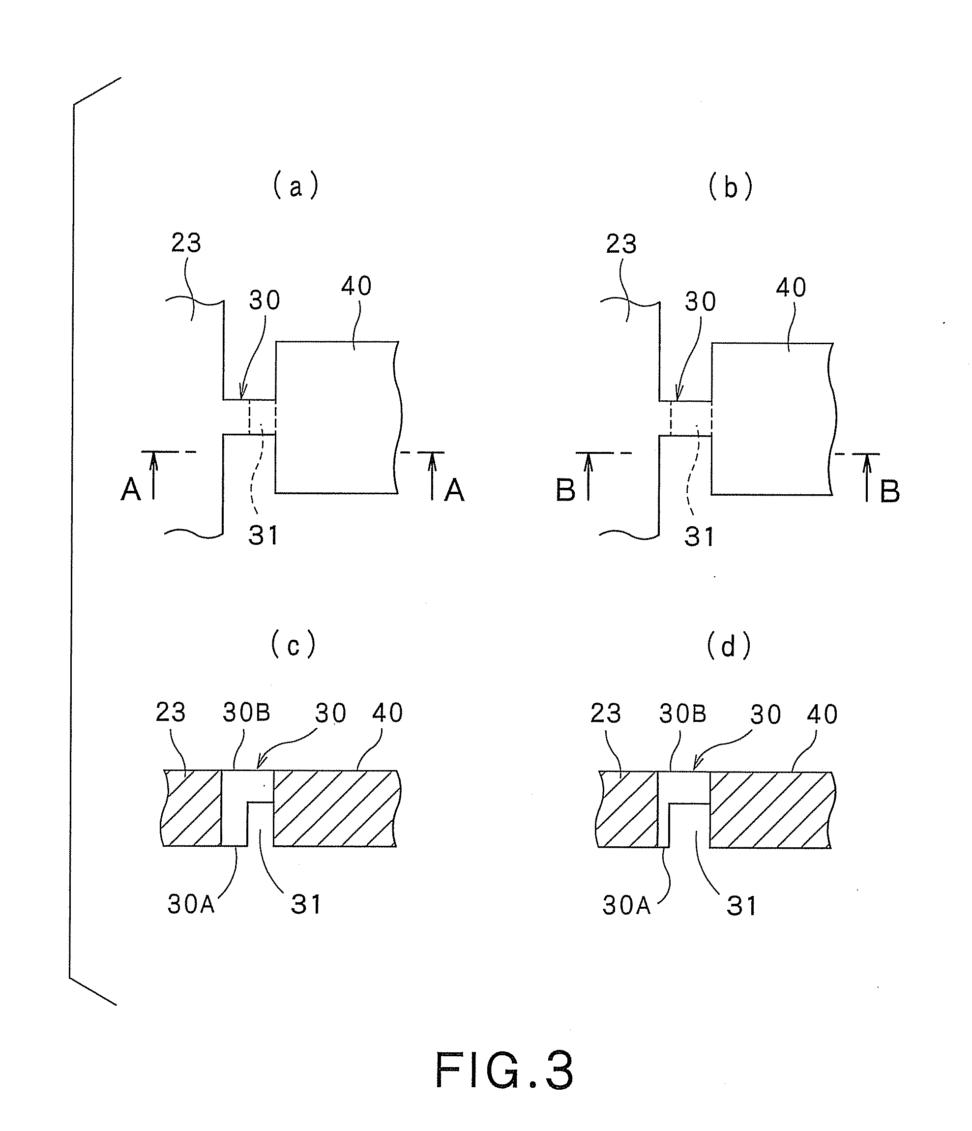
[0060]As shown in FIG. 1, the metallic shielding sheet 10 includes a frame body 20 having a plurality of rectangular openings 21, and a plurality of metallic shielding plates 40 arranged in the openings 21 of the frame body 20 and connected to the frame body 20 via connecting portions 30. The frame body 20 includes an outer frame 22 that surrounds the plurality of entire openings 21, and a plurality of elongated stays 23 formed between mutually adjacent openings 21 and arranged in parallel to one another. The outer frame 22 and stays 23 of the frame body 20, and the metallic shielding plates 40 are the same in thickness between one another.

[00...

second embodiment

[0144]Hereunder, a second embodiment of the present invention will be described with reference made to the accompanying drawings. FIGS. 24 to 33 illustrate the second embodiment of the present invention.

(Semiconductor Device Configurations)

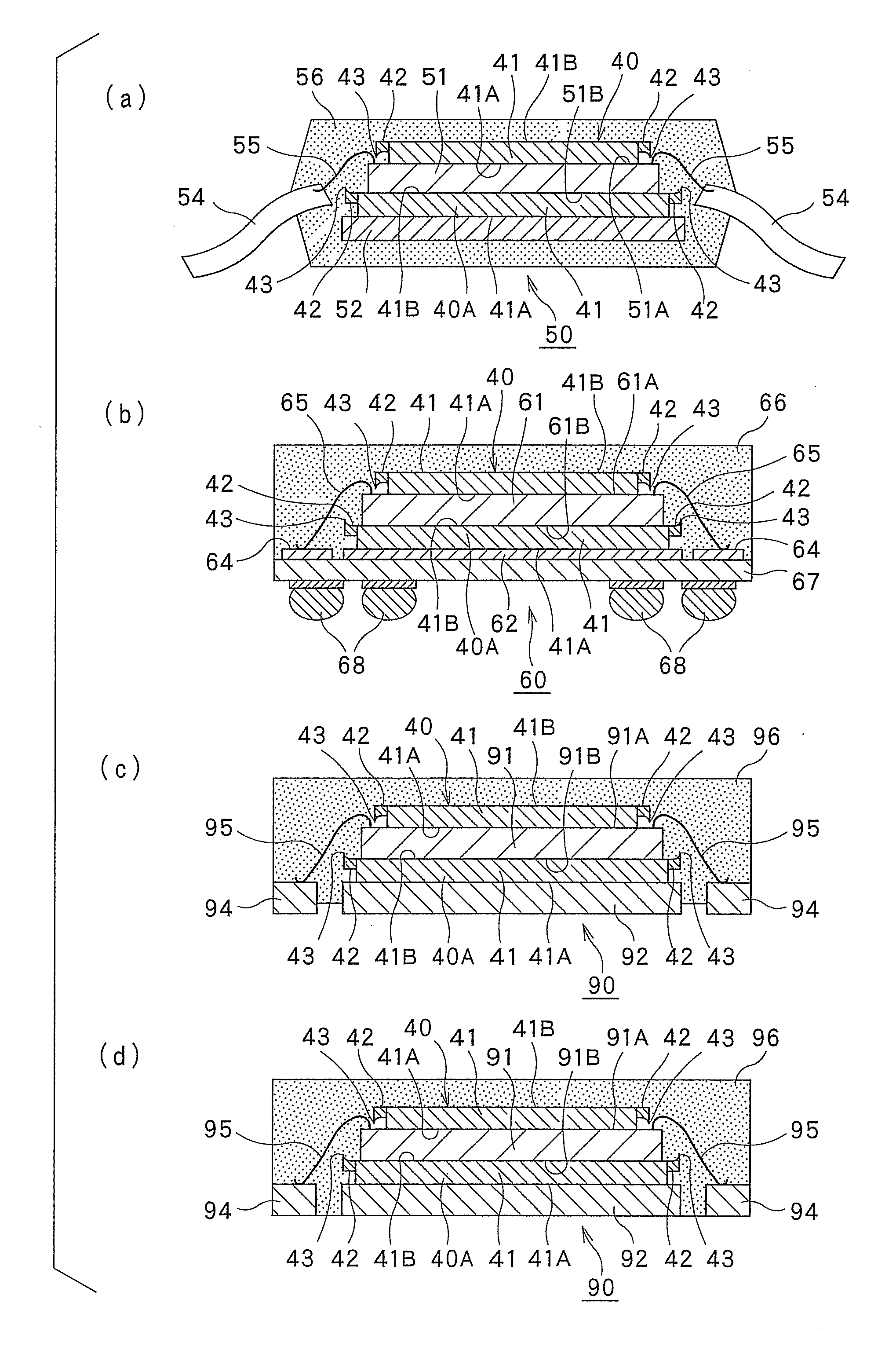
[0145]First, semiconductor devices with a metallic shielding plate are outlined below in accordance with FIGS. 24 to 27. FIGS. 24 and 26 illustrate semiconductor devices formed as SOPs (short for Small Outline Packages), and FIGS. 25 and 27 illustrate semiconductor devices formed as BGAs (short for Ball GridArray Packages).

[0146]The SOP type of semiconductor device shown in FIG. 24 includes a die pad 52, a semiconductor chip 51 mounted on the die pad 52 and having a circuit surface 51A, and a metallic shielding plate 40 provided on the circuit surface 51A of the semiconductor chip 51. The semiconductor chip 51 includes a semiconductor memory such as an MRAM, inclusive of a storage element that exhibits a magnetoresistive effect.

[0147]The metallic ...

example

[0192]The following describes a more specific example of implementing the present invention:

[0193]First, a flat-plate-like permalloy PC material 70 with a plate thickness “t” of 0.150 mm is set in place. Next, the permalloy PC material 70 is worked by etching. More specifically, after plate make-up using an original plate designed so that connections 30 are thinly formed by half-etching, a plurality of flat-plate-like worked permalloy PC materials 10 are fabricated that each include metallic shielding plates 40.

[0194]Next, the plurality of worked flat-plate-like permalloy PC materials 10 are arranged in stacked form in a heat-treating furnace (electric furnace) 110 and then heat-treated at 750° C. in an inert gas (hydrogen gas) atmosphere. Prior to the heat treatment, a spacer 111 is interposed between the flat-plate-like worked permalloy PC materials 10.

[0195]After thus being heated at 750° C. for four hours, the worked permalloy PC materials 10 are gradually cooled (annealed). The...


PUM

PropertyMeasurementUnit
Temperatureaaaaaaaaaa
Metallic bondaaaaaaaaaa

Abstract

Provided is a semiconductor device capable of preventing a semiconductor chip from being damaged by any sharp burrs of a metallic shielding plate. The semiconductor device includes a semiconductor chip and a metallic shielding plate provided on a circuit surface of the semiconductor chip. The metallic shielding plate is disposed in such a manner that a second surface of a shielding plate body is directed towards the circuit surface of the semiconductor chip, and burrs are positioned contiguous to the second surface of the shielding plate body. At distal ends of the burrs, cutting burrs are formed in a direction orthogonal to the second surface. The sharp burrs extend in a direction opposite to the semiconductor chip, so that the sharp burrs are prevented from damaging the circuit surface of the semiconductor chip.

Description

CROSS-REFERENCE TO RELATED APPLICATIONS[0001]The present patent application benefits from Japanese Patent Application No. 2009-109369 filed on Apr. 28, 2009, and Japanese Patent Application No. 2009-136462 filed on Jun. 5, 2009, the entire content of which is hereby incorporated by reference into the present application.BACKGROUND OF THE INVENTION[0002]1. Field of the Invention[0003]The present invention relates generally to semiconductor devices having a metallic shielding plate to protect a semiconductor chip from magnetism. More particularly, the invention is directed to a semiconductor device capable of preventing a semiconductor chip from becoming damaged by contact with any burrs formed at edges of a metallic shielding plate during cutting thereof. The invention also concerns a method of manufacturing a metallic shielding plate used in a semiconductor device including a semiconductor chip and a resin for sealing the semiconductor chip, the metallic shielding plate protecting t...

Claims


Application Information

Patent Timeline
IPC IPC(8): H01L23/58H01F41/00
CPCH01L23/16H01L23/3107H01L23/495H01L23/552H01L24/29H01L24/45H01L24/48H01L2224/29339H01L2224/32225H01L2224/32245H01L2224/45144H01L2224/48091H01L2224/48227H01L2224/48247H01L2224/49171H01L2224/73265H01L2224/83101H01L2924/01079H01L2924/15311H01L2924/3025H01L24/49H01L2924/01013H01L2924/01028H01L2224/27013Y10T29/49002H01L2924/00014H01L2924/00H01L2924/00012H01L24/73H01L2924/181
Inventor MASUDA, MASACHIKAODA, KAZUNORITOMITA, KOJIMIYANO, KAZUYUKI
Owner DAI NIPPON PRINTING CO LTD
Why Eureka
Try Eureka