Semiconductor chip and method of fabricating the same

Inactive Publication Date: 2006-08-24
RENESAS ELECTRONICS CORP
View PDF3 Cites 9 Cited by
  • Summary
  • Abstract
  • Description
  • Claims
  • Application Information

AI Technical Summary

Benefits of technology

[0043] The fuse residue may be formed on the same plane with the fuse. An insulating film may be formed on the fuse residue and the fuse. The fuse residue can be configured as being covered with the insulating film on the top portion and side faces thereof. Even for the case where the fuse residue has a geometry in which the patterns corresponded to a part of the blowable region are connected to both patterns corresponded to the first terminal and the second terminal, the patterns corresponded to a part of the blowable region are isolated from each other by the insulating film. This configuration can avoid short-circuiting when a detection is made by a fuse detection circuit on whether the fuse residue has been blow or not.
[0044] The semiconductor chip of the present invention includes the preliminarily-disconnected, fuse-like fuse residue, and the fuse, so that the logic circuits of the semiconductor chip can be configured in a programmable manner by blowing the fuse when the situation demands. The fuse residue has no blow mark, so that it is al

Problems solved by technology

The technique disclosed in WO98/09327 is, however, aimed at efficiently fabricate the gate array using the anti-fuse-system FPGA, having the same logic functions therewith, and thus-fabricated gate array has no fuses formed therein, so that

Method used


Image

  • Semiconductor chip and method of fabricating the same
  • Semiconductor chip and method of fabricating the same
  • Semiconductor chip and method of fabricating the same

Examples


Example

First Embodiment

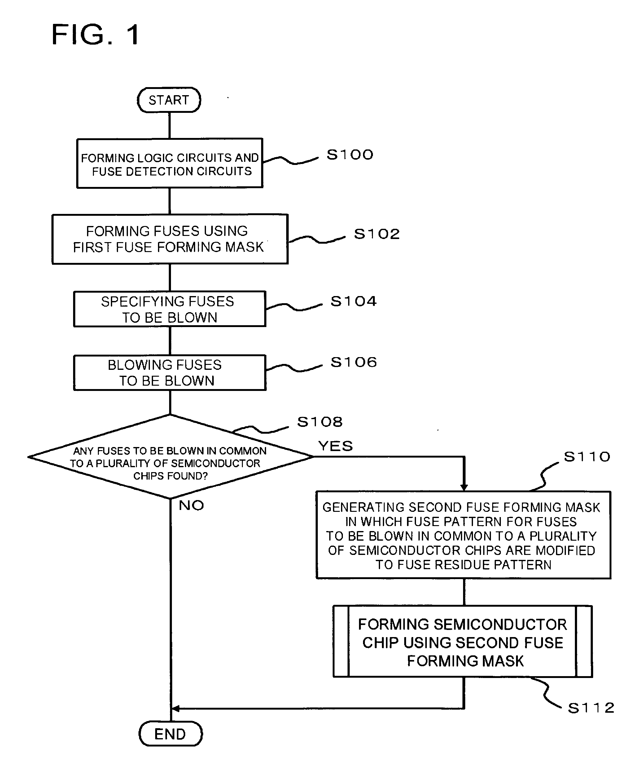
[0079] The first embodiment will be described exemplifying a fuse used for regulating voltage between two logic circuits.

[0080]FIG. 3 is a top view showing a configuration of the first fuse-forming mask used in step S102 in FIG. 1.

[0081] The first fuse-forming mask 220 has a plurality of fuse patterns 132 formed thereon. Each fuse pattern 132 includes a first terminal pattern 134, a blowable region pattern 136, and a second terminal pattern 138. The fuse pattern 132 may have other various geometries, without being limited to the geometry shown herein.

[0082]FIG. 4 is a schematic top view showing a configuration of the first semiconductor chip 200 formed by using the first fuse-forming mask 220 shown in FIG. 3.

[0083] The first semiconductor chip 200 includes a plurality of fuses 106. Each fuse 106 includes a first terminal 108, a second terminal 112, and a blowable region 110 electrically connected thereto and disposed therebetween. In the first embodiment, blowab...

Example

Second Embodiment

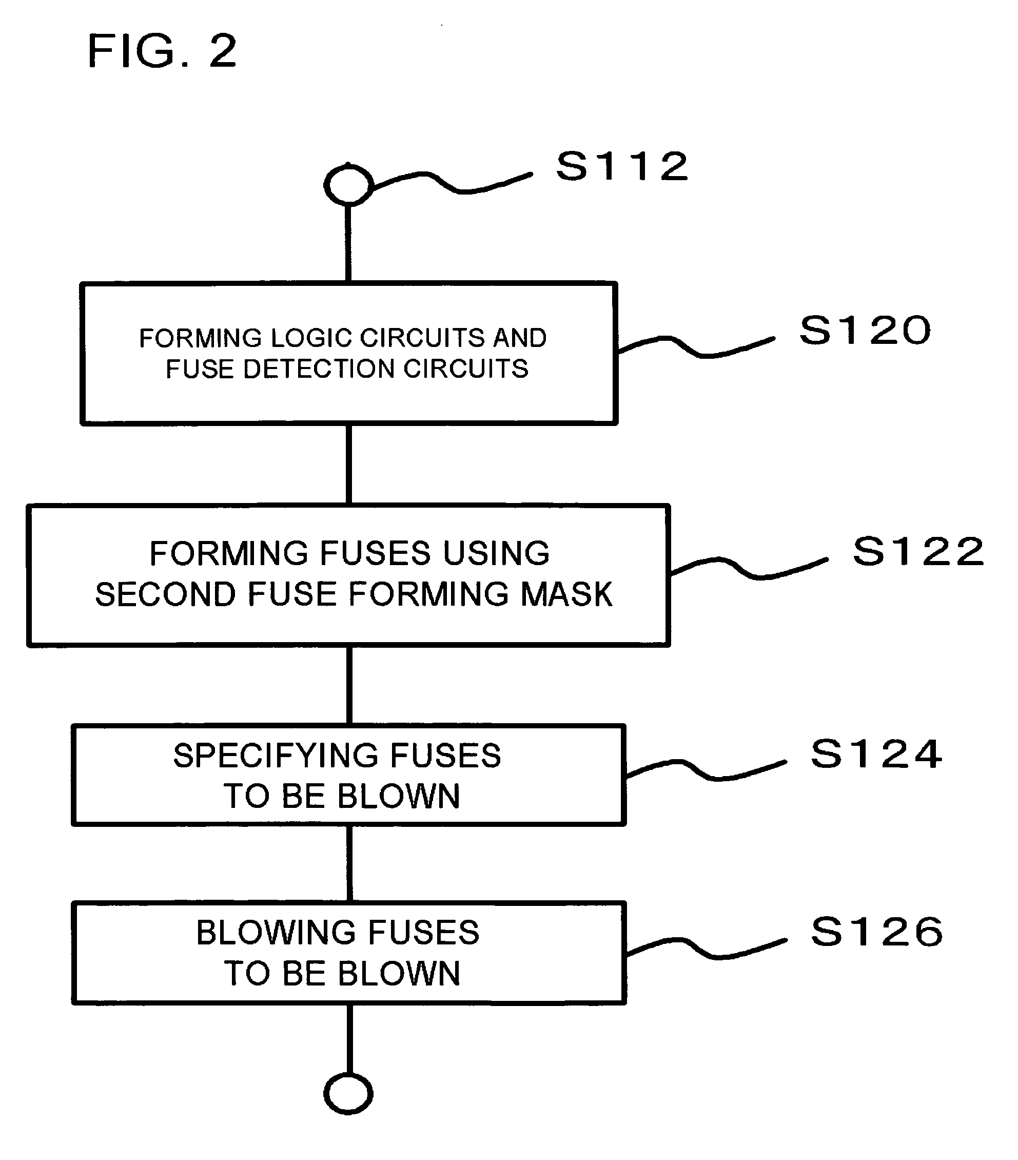
[0124] Also in the second embodiment, fuses regulating voltage between two logic circuits will be described similarly to as in the first embodiment. In the second embodiment, the geometry of the fuse residues 118 differ from that in the first embodiment.

[0125]FIG. 12 is a top view showing a configuration of the second fuse-forming mask 130 in the second embodiment.

[0126] The first fuse residue pattern 141 of the fuse residue pattern 140 in the second embodiment has, in addition to a pattern same as that of the first terminal pattern 134 of the fuse pattern 132, a pattern same as that of a part of the blowable region pattern 136. The second fuse residue pattern 142 of the fuse residue pattern 140 has, in addition to a pattern same as that of the second terminal pattern 138 of the fuse pattern 132, a pattern same as that of a part of the blowable region pattern 136. The first fuse residue pattern 141 and the second fuse residue pattern 142 herein are not connected ...

Example

Third Embodiment

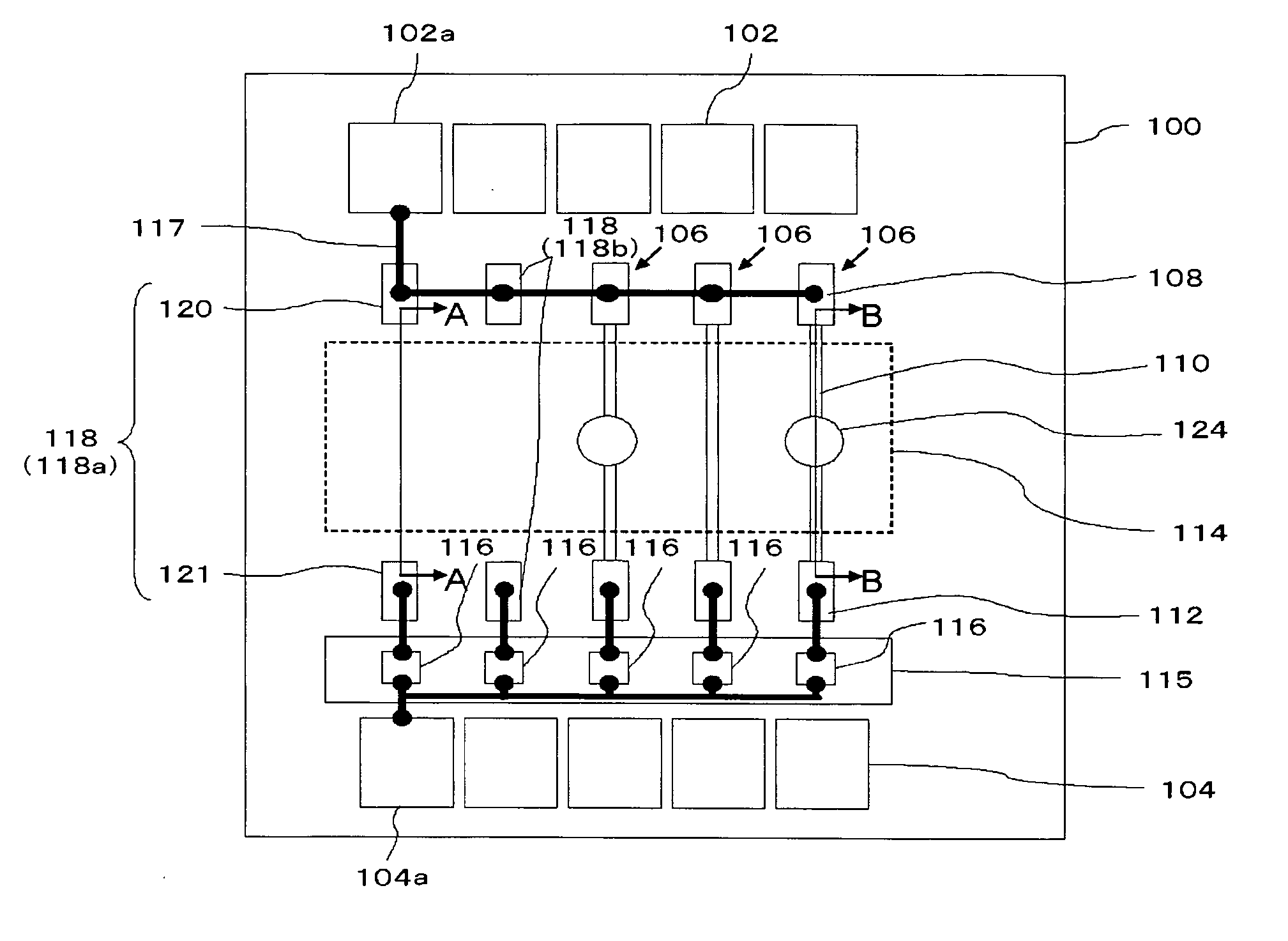
[0135] Also in the third embodiment, fuses regulating voltage between two logic circuits will be described similarly to as in the first and second embodiments. The third embodiment differs from the first embodiment and the second embodiment, in that the fuses 106 are blown by current supply.

[0136]FIG. 16 is a schematic top view showing a configuration of the second semiconductor chip 100 in which the fuses 106 to be blown are blown by current supply, rather than laser irradiation.

[0137] In the third embodiment, the second semiconductor chip 100 further includes a current generation circuit 119. The target fuses 106 can be blown by being supplied with current generated by the current generation circuit 119.

[0138]FIG. 17 is a sectional view taken along line D-D in FIG. 16.

[0139] In the third embodiment, there is no need of forming the fuse blowing recess 114 to the second insulating film 156 and the polyimide film 158. The blowable region 110 can electrically be d...


PUM


Abstract

There is provided a semiconductor chip having fuses. The semiconductor chip includes fuses each having a first terminal electrically connected to a first logic circuit, a second terminal electrically connected to a second logic circuit, and a blowable region formed between the first terminal and the second terminal; and fuse residues each having the same patterns with those of the first terminal and the second terminal of the fuses, and configured so that patterns corresponded to the first terminals and the second terminals are electrically disconnected from each other.

Description

[0001] This application is based on Japanese patent application No. 2005-048523 the content of which is incorporated hereinto by reference. BACKGROUND [0002] 1. Technical Field [0003] The present invention relates to a semiconductor chip having fuses, and a method of fabricating the same. [0004] 2. Related Art [0005] Fuses are introduced into semiconductor devices for various purposes. Memories such as DRAM, for example, introduce the fuses for the purpose of redundancy replacement by which a redundant bit is allowed to operate in place of a fault bit (K. Arndt et al., Reliability of Laser Activated Metal Fuses in DRAMs, 1999 IEEE / CPMT Int'l Electronics Manufacturing Technology Symposium, p. 389-394). In this case, operations of a semiconductor device are tested after the wafer process, and if any fault bit is found, a fuse connected to the fault bit is blown in order to replace such fault bit with a redundant bit. [0006] The fuses are also introduced among a plurality of target log...

Claims


Application Information

Patent Timeline
IPC IPC(8): H01L21/82
CPCH01L27/11803
Inventor SAKOH, TAKASHIKUBOTA, RYO
Owner RENESAS ELECTRONICS CORP
Why Eureka
Try Eureka