Input device and display device having the same

a display device and input device technology, applied in the field of input devices, can solve the problems of user discomfort when inputting characters, increased cost, etc., and achieve the effects of deteriorating image quality of the display device, reducing the distance between the z electrode and the x electrode, and increasing the electrostatic capacitance therebetween

Inactive Publication Date: 2010-10-28
JAPAN DISPLAY INC +1
View PDF10 Cites 30 Cited by
  • Summary
  • Abstract
  • Description
  • Claims
  • Application Information

AI Technical Summary

Benefits of technology

[0012]In order to solve the above-mentioned problems, according to a first aspect of the present invention, an electrostatic capacitive coupling-type touch panel is used which includes a plurality of transparent X electrodes, a plurality of transparent Y electrodes, and transparent Z electrodes. In the electrostatic capacitive coupling-type touch panel, the X electrodes and the Y electrodes intersect each other with a first insulating layer disposed therebetween and each have a configuration in which a pad part and a thin line part alternate in their extending direction. The pad parts of the X electrodes and the pad parts of the Y electrodes are arranged so as not to overlap each other in plan view. The Z electrodes are arranged over the X electrodes and the Y electrodes with spacers disposed therebetween for maintaining a constant distance and The Z electrodes are deformed along the shape of the spacers by compressive force resulting from touch pressing. In this way, the distance between the Z electrodes and the X electrodes and the distance between the Z electrodes and the Y electrodes are decreased, and accordingly, the electrostatic capacitance therebetween is increased. Therefore, it is possible to detect the coordinates of the touched position with non-conductive input means by detecting a capacitance change between the X and Y electrodes and the Z electrodes (portions where an inter-electrode distance is changed by the pressing).
[0013]Moreover, according to a second aspect of the present invention, the Z electrodes are arranged over the X electrodes and the Y electrodes with a plurality of dot-shaped elastic spacers disposed therebetween for maintaining a constant distance, and the elastic spacers are deformed by compressive force resulting from the touch pressing. The Z electrodes may be arranged with a spongy layer similar to the dot-shaped elastic spacers. However, the spongy layer may cause diffused reflection of light and lead to deterioration in image quality of the display device. Thus, the dot-shaped elastic spacers are preferable. By the elastic spacers, the distance between the Z electrodes and the X electrodes and the distance between the Z electrodes and the Y electrodes are decreased, and accordingly, the electrostatic capacitance therebetween is increased. Moreover, an insulating layer may be provided between the Z electrodes and the X and Y electrodes in order to detect the electrostatic capacitance that changes in response to the decrease in the distance between the Z electrodes and the X electrodes and the distance between the Z electrodes and the Y electrodes. Therefore, by providing an anti-reflection film at an interface between the space (air layer) formed by the elastic spacers and a stacked structure adjacent to the space, the transmittance can be improved and on-screen reflection can be reduced, thus suppressing deterioration in the image quality of the display device. Accordingly, it is possible to detect a capacitance change between the X and Y electrodes and the Z electrodes (portions where an inter-electrode distance is changed by the pressing) with non-conductive input means and thus to identify the coordinates of the touched position.

Problems solved by technology

Furthermore, since the circuit area also increases due to the increase in the number of terminals of the input processing unit, the costs may also increase.
Thus, users may experience discomfort when inputting characters.
From the above, the electrostatic capacitive coupling-type touch panel disclosed in Patent Document 1 has a problem in dealing with input operations using an insulating material (stylus).

Method used


Image

  • Input device and display device having the same
  • Input device and display device having the same
  • Input device and display device having the same

Examples


first embodiment

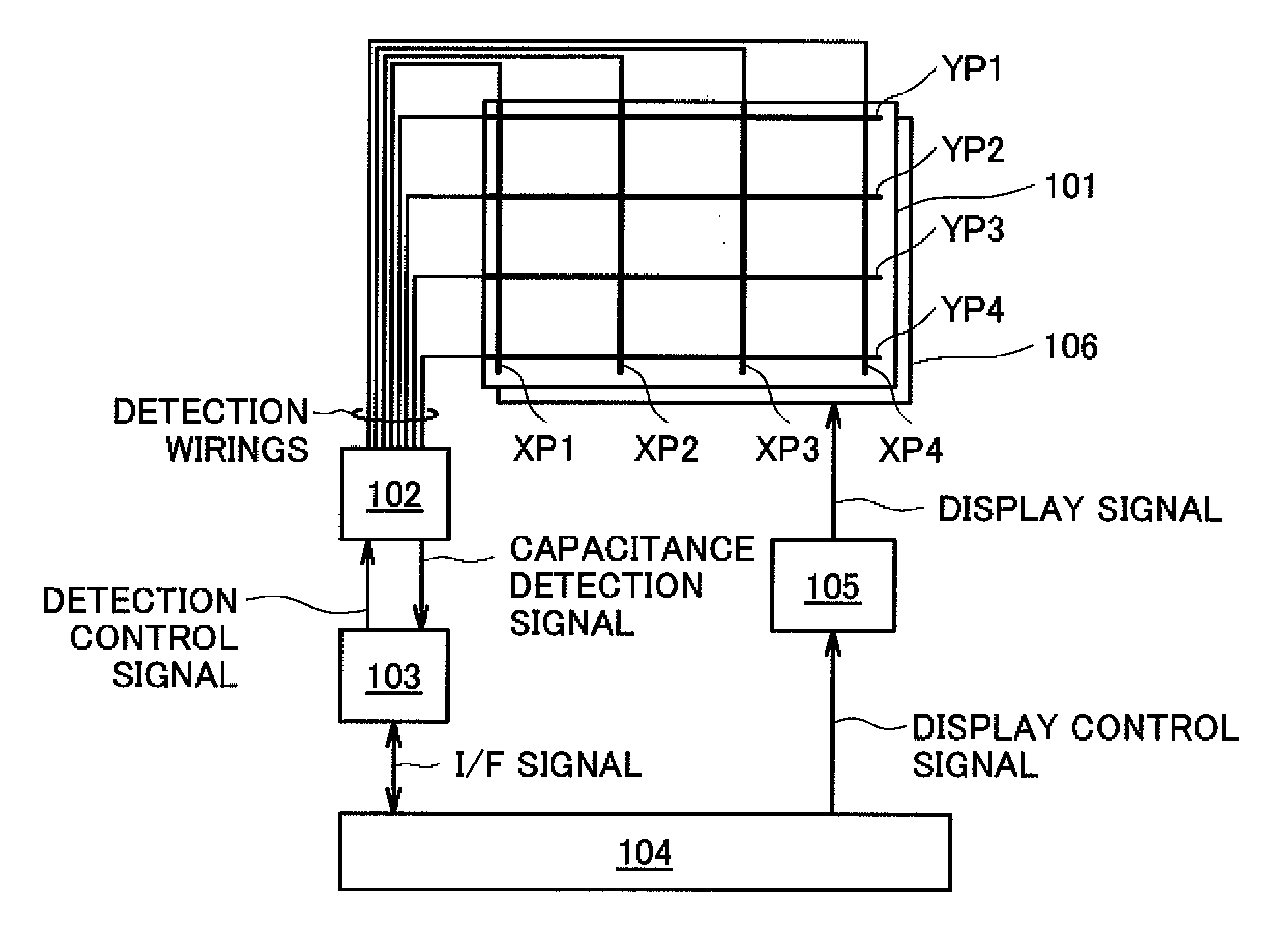
[0033]The configuration of an input device (hereinafter referred to as a touch panel) and a display device having the same is shown in FIG. 1.

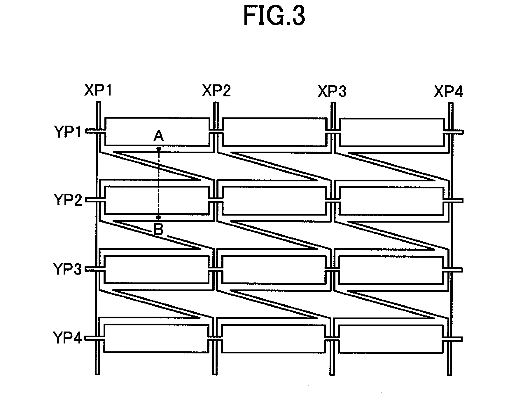
[0034]In FIG. 1, reference numeral 101 denotes a touch panel according to the embodiments of the present invention. The touch panel 101 includes X and Y electrodes XP and YP for capacitance detection. Although four X electrodes XP1 to XP4 and four Y electrodes YP1 to YP4 are shown in this example, the number of the electrodes is not limited to this. FIG. 5 shows a layout diagram of the X and Y electrodes for capacitance detection of a touch panel that has a diagonal size of 4 inches (its aspect ratio is assumed to be 3:4), for example.

[0035]The touch panel 101 is installed on a front face of a display portion 106 of the display device. It is therefore desirable for the touch panel 101 to have high transmittance since when a user views an image displayed on the display device, the displayed image must be transmitted through the touch panel 101....

second embodiment

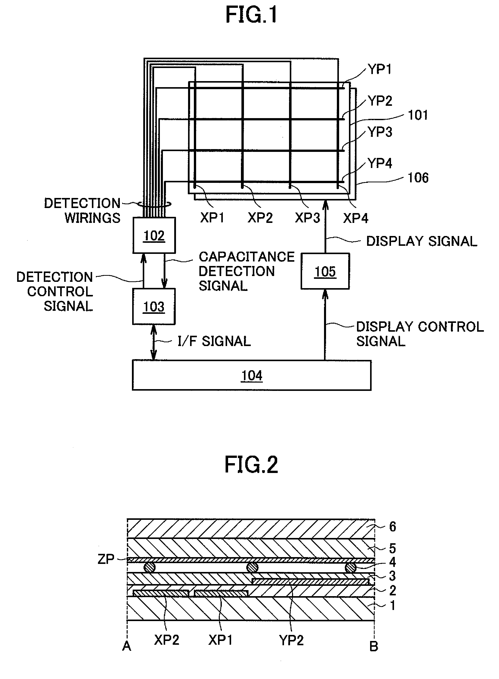
[0053]FIG. 6 is a configuration diagram of a touch panel 101 according to a second embodiment of the present invention and shows the sectional shape of the touch panel 101 taken along the line A-B in FIG. 3. The materials and properties of the respective layers are the same as those of the first embodiment, and description thereof will be omitted herein.

[0054]The touch panel 101 of the present embodiment has a stacked structure in which a transparent conductive film XP, a first transparent insulating film 2, a transparent conductive film YP, a second transparent insulating film 3, a transparent elastic layer 5, a Z electrode ZP, spacers 4 for maintaining a distance to the Z electrode, and a second transparent substrate 6 are successively stacked in that order on a first transparent substrate 1.

[0055]Next, a capacitance change when a touch operation is made on the touch panel 101 according to the second embodiment of the present invention will be described with reference to FIG. 7.

[0...

third embodiment

[0062]FIG. 8 is a configuration diagram of a touch panel 101 according to a third embodiment of the present invention and shows the sectional shape of the touch panel 101 taken along the line A-B in FIG. 3.

[0063]The touch panel 101 of the present embodiment has a stacked structure in which a transparent conductive film XP, a first transparent insulating film 2, a transparent conductive film YP, a second transparent insulating film 3, spacers 4 for maintaining a distance to a Z electrode, the Z electrode ZP, a transparent elastic layer 5, and a second transparent substrate 6 are successively stacked in that order on a first transparent substrate 1.

[0064]The spacers 4 are made of a light-curable resin material and can be configured as dot-shaped pillar spacers. The spacers 4 are preferably formed at intervals of 20 μm or more and 10000 μm or less by a screen printing method or the like. The spacers 4 may have a circular or rectangular shape and have a diameter of 5 to 100 μm, and pref...


PUM


Abstract

An electrostatic capacitive coupling-type touch panel is provided which interacts not only with a finger-based input but also with a touch using non-conductive input means. The touch panel includes coordinate detection electrodes for detecting XY position coordinates and transparent Z electrodes. The Z electrodes are arranged over the coordinate detection electrodes at certain intervals with spacers disposed therebetween. An elastic layer that is deformed along the shape of the spacers by compressive force resulting from touch pressing presses the Z electrodes.

Description

CROSS-REFERENCE TO RELATED APPLICATION[0001]The present application claims priority from Japanese applications JP2009-103495 filed on Apr. 22, 2009 and JP2009-267325 filed on Nov. 25, 2009, the contents of which are hereby incorporated by reference into these applications.BACKGROUND OF THE INVENTION[0002]1. Field of the Invention[0003]The present invention relates to an input device for inputting coordinates to a screen and a display device having the same, and more particularly, to a capacitive-coupling input device capable of inputting coordinates using a plastic pen or the like, which is an insulator, and a display device having the same.[0004]2. Description of Related Art[0005]A display device having an input device (hereinafter also referred to as a “touch sensor” or a “touch panel”) having an on-screen input function of inputting information to a display screen by a touch operation (a contact and press operation; hereinafter simply referred to as a “touch”) with a user's finge...

Claims


Application Information

Patent Timeline
Patent Type & Authority Applications(United States)
IPC IPC(8): G06F3/045
CPCG06F3/044G06F3/0412G06F3/0445G06F3/0446G06F3/0447
Inventor SEKIGUCHI, SHINJINAGATA, KOJIHAYAKAWA, KOUJIMAMBA, NORIO
Owner JAPAN DISPLAY INC
Why Eureka
Try Eureka