Accessing Memory Cells in a Memory Circuit

a memory circuit and memory cell technology, applied in the field of memory circuits, can solve the problems of increasing power consumption in the memory circuit, degrading performance, and affecting so as to reduce the read access time and reduce the overall performance of the memory circuit. the effect of degrading the overall performance of the memory circui

Active Publication Date: 2010-10-28
LSI CORPORATION
View PDF2 Cites 35 Cited by
  • Summary
  • Abstract
  • Description
  • Claims
  • Application Information

AI Technical Summary

Benefits of technology

[0006]Illustrative embodiments of the present invention provide techniques for beneficially accessing weak memory cells in a memory circuit without degrading the overall performance of the memory circuit. To accomplish this, embodiments of the invention selectively modify one or more control parameters used in operating weak memory cells when accessing the weak cells compared to control parameters used for operating normal memory cells. Modifications to the weak cell control parameters may be a function of certain characteristics of the weak cells, such as, for exa

Problems solved by technology

Such variations and/or defects in a memory circuit may result in some memory cells taking longer to read or write than other cells, or some memory cells requiring higher voltage or power to read or write than other cells.
Unfortunately, however, setting memory circuit operational parameters to accommodate all memory cells, including weak cells, has a disadvantage of degrading performance of the majority of memory cells in the memory circuit, and using higher operating voltage than is necessary for proper functioning of the majority of memory

Method used


Image

  • Accessing Memory Cells in a Memory Circuit
  • Accessing Memory Cells in a Memory Circuit
  • Accessing Memory Cells in a Memory Circuit

Examples


Embodiment Construction

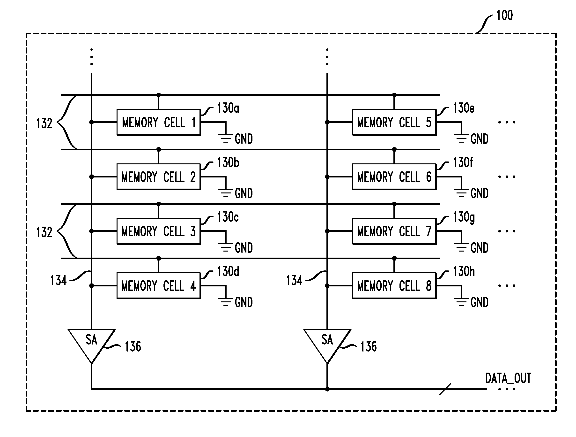
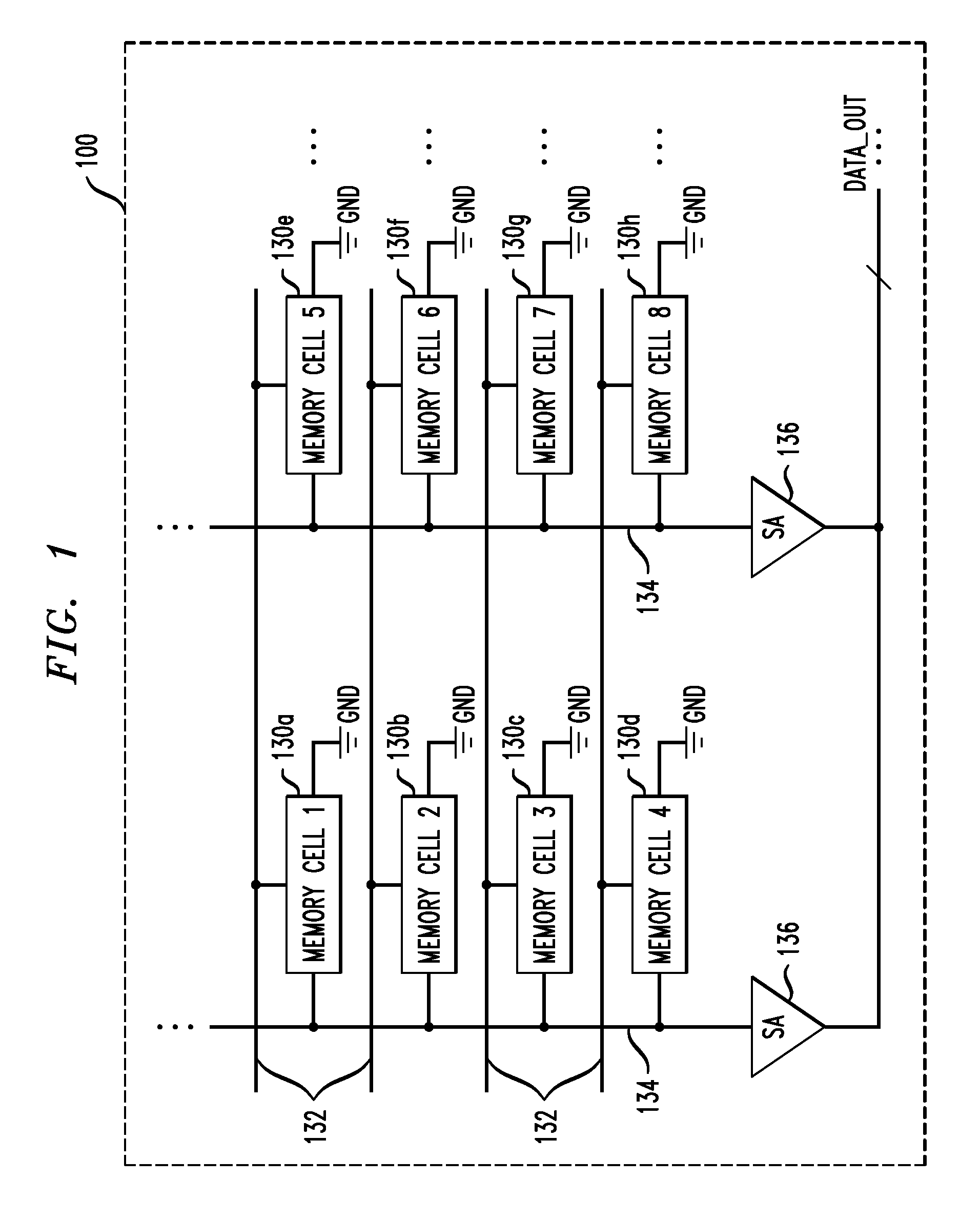
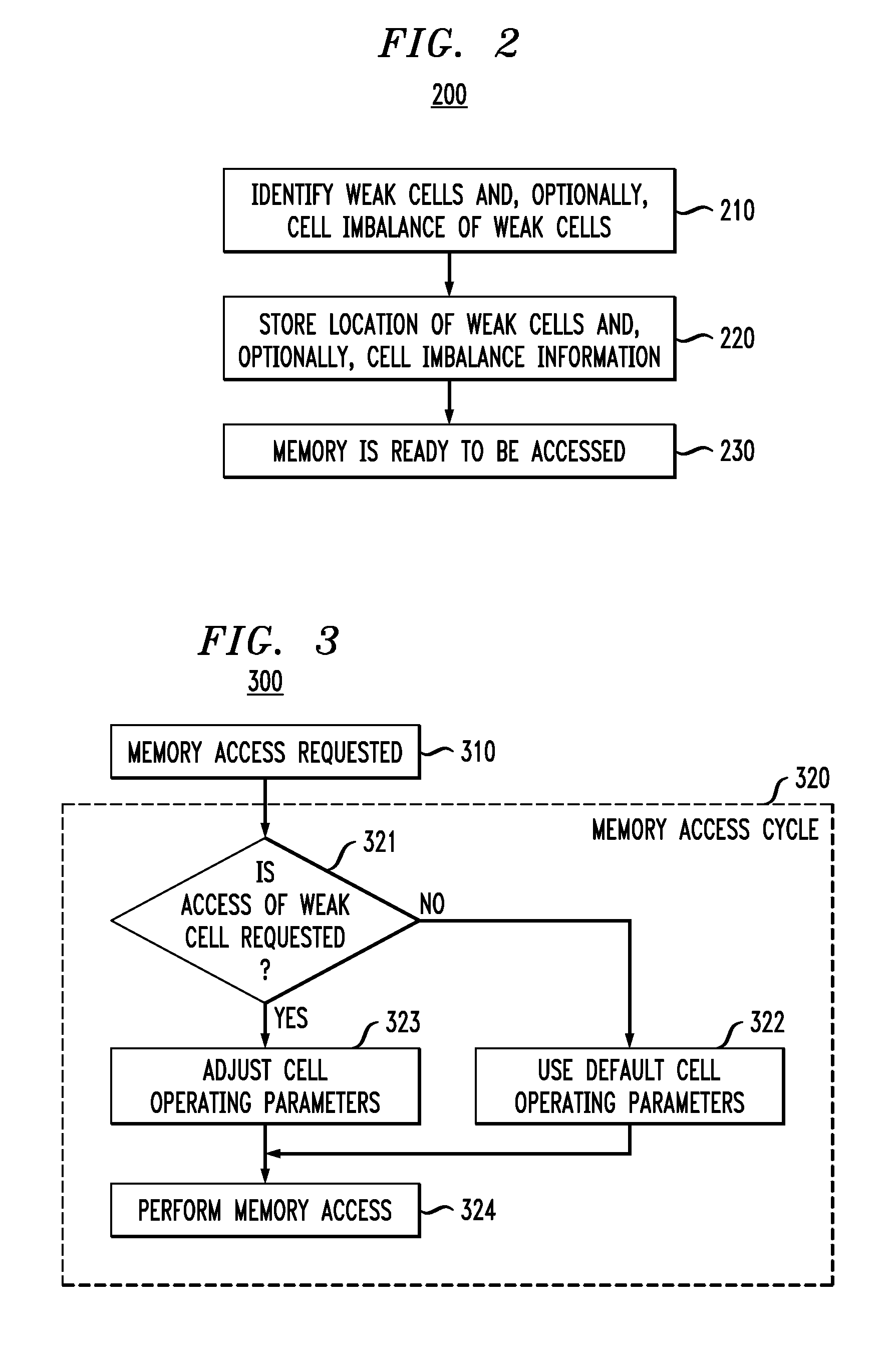
[0016]The present invention will be described herein in the context of illustrative embodiments of a memory circuit and methods for accessing a memory circuit having weak memory cells. It is to be appreciated, however, that the techniques of the present invention are not limited to the specific circuit and methods shown and described herein. Rather, embodiments of the invention are directed broadly to improved techniques for ensuring proper operation of weak memory cells in a memory circuit without undesirably operating all of the memory cells in the memory circuit using timing, voltage, and / or other parameters of the weak cells and without incurring the relatively high cost of providing memory cell redundancy. For this reason, numerous modifications can be made to the embodiments shown that are be within the scope of the present invention. Moreover, although preferred embodiments of the invention are preferably fabricated in a silicon wafer, embodiments of the invention can alterna...


PUM


Abstract

Techniques for accessing a memory cell in a memory circuit include: receiving a request to access a selected memory cell in the memory circuit; determining whether the selected memory cell corresponds to a normal memory cell or a weak memory cell in the memory circuit; accessing the selected memory cell using a first set of control parameters when the selected memory cell corresponds to a normal memory cell, wherein the selected memory cell provides correct data under prescribed operating specifications when accessed using the first set of control parameters; and accessing the selected memory cell using a second set of control parameters when the selected memory cell corresponds to a weak memory cell, wherein the selected memory cell provides correct data under the prescribed operating specifications when accessed using the second set of control parameters and provides incorrect data under the prescribed operating specifications when accessed using the first set of control parameters.

Description

FIELD OF THE INVENTION[0001]The present invention relates generally to the electrical, electronic, and computer arts, and more particularly relates to memory circuits.BACKGROUND OF THE INVENTION[0002]Memory circuits, including those embedded in integrated circuits (ICs), are of various known types, including, but not limited to, dynamic random access memory (DRAM), static random access memory (SRAM), read only memory (ROM), and other non-volatile memories such as flash memory, phase-change memory (PCM), one-time-programmable (OTP) memory, and few-time-programmable (FTP) memory. Memory circuits typically comprise an array of memory storage cells, sometimes having as many as tens of millions of memory cells or more (e.g., megabits of storage).[0003]Regardless of memory type, variations often occur within memory circuits, generally between otherwise identical memory cells in a memory array. Defective memory cells can also occur. Statistically, the larger the number of memory cells in t...

Claims


Application Information

Patent Timeline
IPC IPC(8): G11C29/00G11C8/00G11C7/00G06F11/00G06F11/27
CPCG11C5/06H01L2225/06568G11C7/24G11C8/10G11C11/4076G11C11/4078G11C29/028G11C29/50G11C29/70G11C29/88G11C2029/1208G11C2029/5002H01L25/0657H01L25/18H01L2224/16145G11C7/22H01L2924/00014H01L2924/00011
Inventor DELL, RICHARD BRUCEKOHLER, ROSS A.MCPARTLAND, RICHARD J.WERNER, WAYNE E.
Owner LSI CORPORATION
Why Eureka
Try Eureka