Polishing apparatus

a technology of polishing apparatus and rotary disc, which is applied in the direction of grinding drives, grinding machine components, manufacturing tools, etc., can solve the problems of insufficient or excessive polishing of the surface of semiconductor wafer in different regions, poor film coating performance (step coverage) over stepped configurations of thin films, and increased manufacturing costs. , to achieve the effect of suppressing thermal expansion reducing the cost of fabrication process, and improving the following capability of the retainer ring

Active Publication Date: 2010-10-28
EBARA CORP
View PDF27 Cites 13 Cited by
  • Summary
  • Abstract
  • Description
  • Claims
  • Application Information

AI Technical Summary

Benefits of technology

[0012]There is a need for a new polishing apparatus capable of coping with these issues thereby reducing cost of fabrication process. Accordingly, there needs an invention to provide a polishing apparatus which can improve the following capability of a retainer ring against a polishing surface, the retainer ring for holding a peripheral edge of a substrate being provided at a peripheral portion of a top ring for holding the substrate, can apply a desired surface pressure of the retainer ring to the polishing surface, and can prevent powder generated at sliding contact portion of the retainer ring from falling down onto the polishing surface and suppress thermal expansion of the retainer ring.

Problems solved by technology

Multilayer interconnections in smaller circuits result in greater steps which reflect surface irregularities on lower interconnection layers.
An increase in the number of interconnection layers makes film coating performance (step coverage) poor over stepped configurations of thin films.
In such polishing apparatus, if the relative pressing force applied between the semiconductor wafer, being polished, and the polishing surface of the polishing pad is not uniform over the entire surface of the semiconductor wafer, then the surface of the semiconductor wafer is polished insufficiently or excessively in different regions thereof depending on the pressing force applied thereto.
In this case, the polishing pad is so elastic that pressing forces applied to a peripheral portion of the semiconductor wafer being polished become non-uniform, and hence only the peripheral portion of the semiconductor wafer may excessively be polished, which is referred to as “edge rounding”.
Thus, the following capability of the retainer ring may become limited and insufficient in some cases, and there is a need for a polishing apparatus that has a capability of allowing a desired surface pressure of the retainer ring to be applied to the polishing surface of the polishing pad.
In the case where such powder falls down onto the polishing surface of a polishing table, defect such as scratch on the semiconductor wafer may be caused by the existence of the powder on the polishing surface in general.
Irrespective of the merit, providing the member (boot) could have a demerit in terms of maintainability, because such boot is required to be reattached at the time of replacement of expendable articles, resulting in the possibility of tedious maintenance.
However, providing too wide clearance may cause an unexpected movement of the retainer ring, and abnormal noise or vibration tends to be generated at the time of collision between the retainer ring guide and the retainer ring caused by movement of the retainer ring in the clearance during polishing.
Further, providing too wide clearance has another deficiency.
4) Heat causes a thermal expansion of the retainer ring, and the heat is caused by friction between the retainer ring and the polishing surface.
If the semiconductor wafer is polished in this state, then the inner circumferential side of the retainer ring is to be worn faster than the outer circumferential side of the retainer ring, resulting in uneven wear of the retainer ring.
Furthermore, uneven wear of the retainer ring could occur and the effect of the retainer ring varies with time due to deformation of the retainer ring caused by a frictional force between the polishing surface and the semiconductor wafer.

Method used


Image

  • Polishing apparatus
  • Polishing apparatus
  • Polishing apparatus

Examples


Embodiment Construction

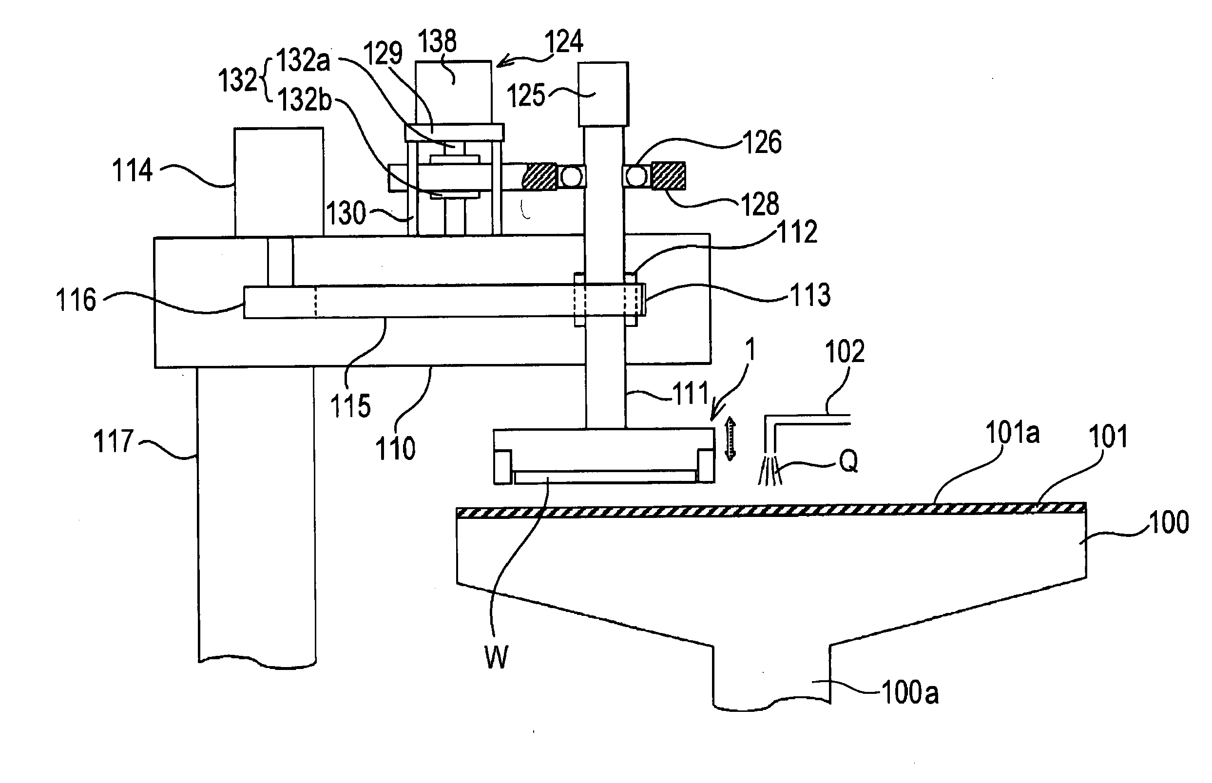
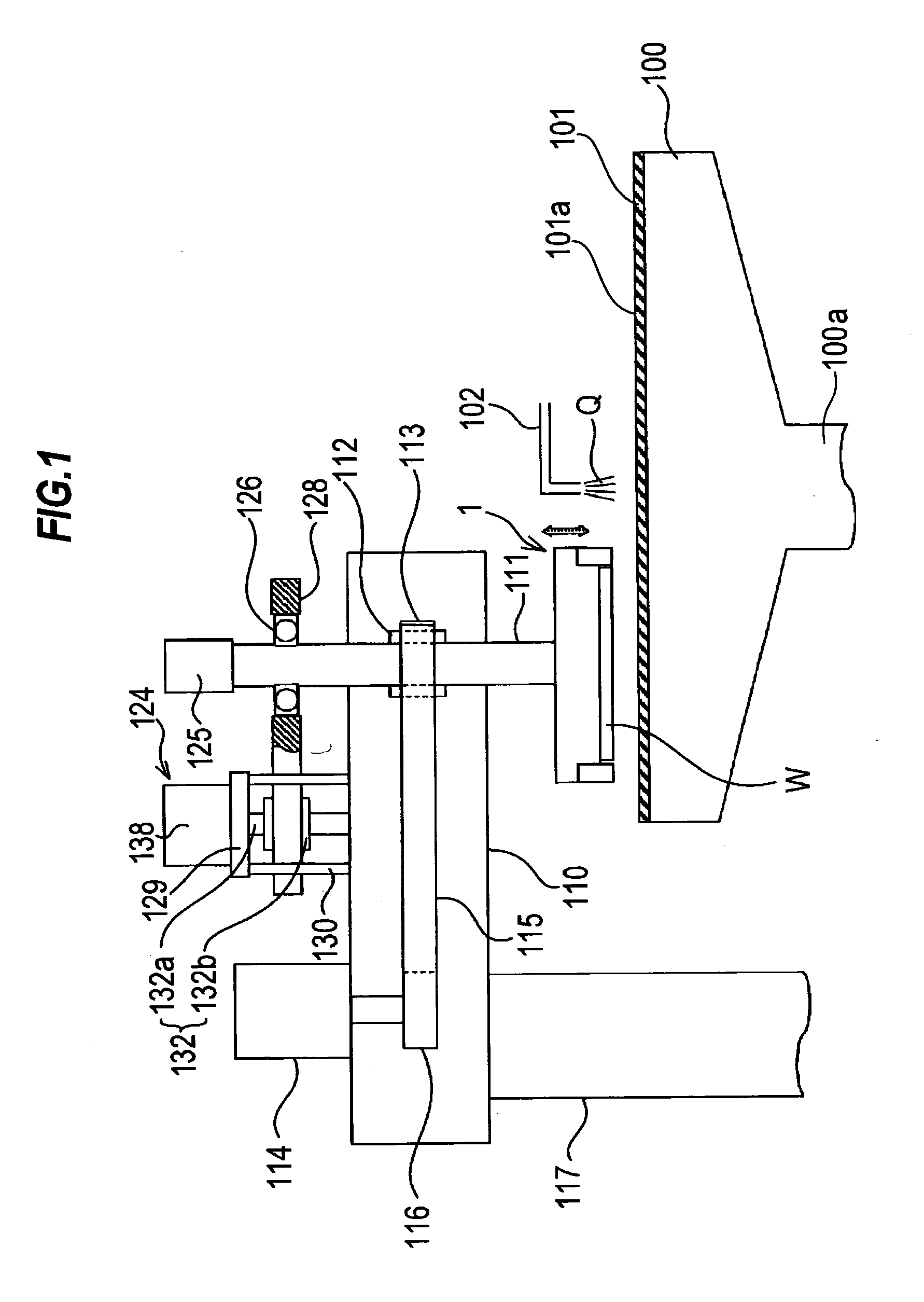
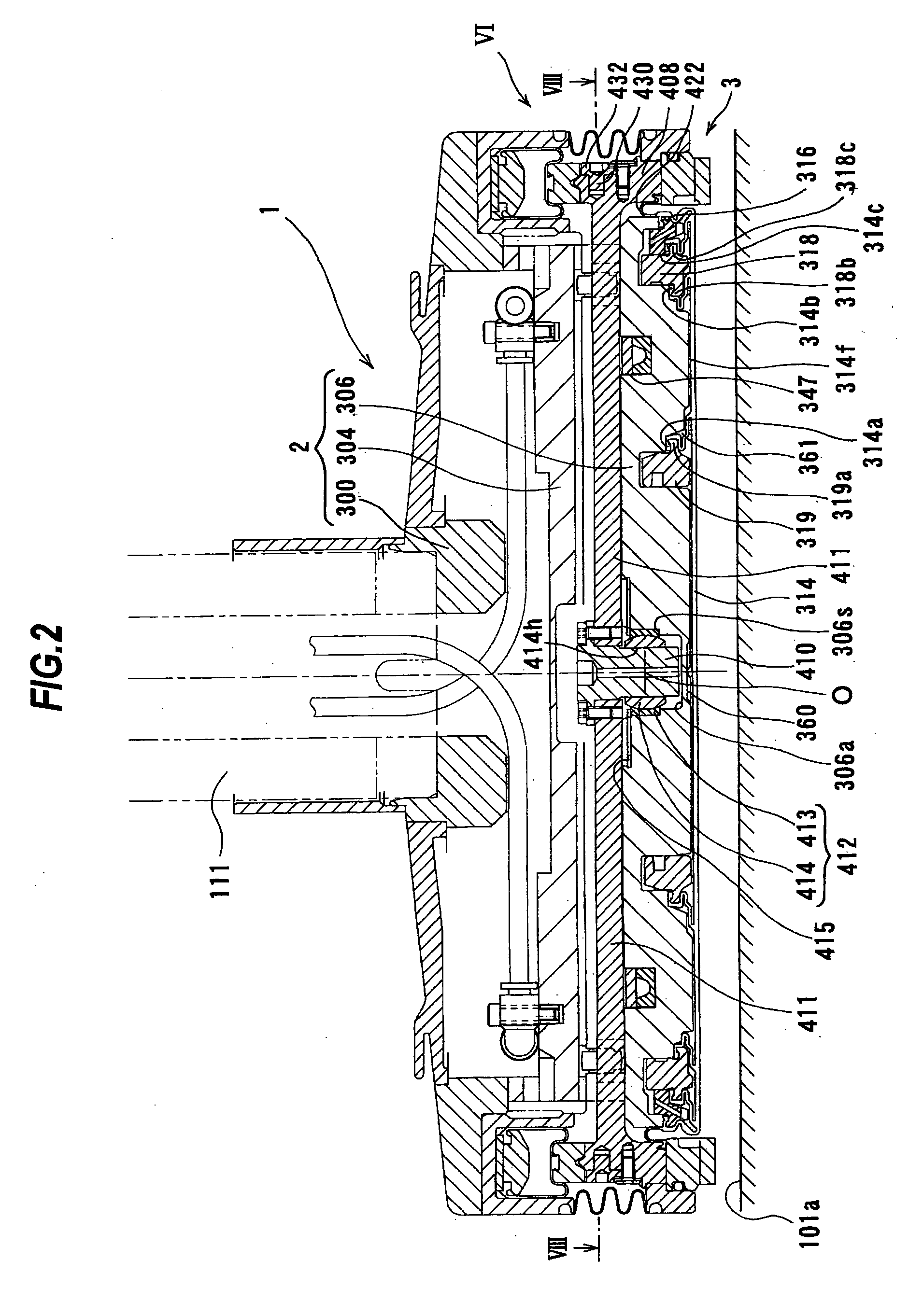
[0063]A polishing apparatus according to embodiments of the present invention will be described below with reference to FIGS. 1 through 19. Like or corresponding parts are denoted by like or corresponding reference numerals throughout drawings and will not be described below repetitively.

[0064]FIG. 1 is a schematic view showing an entire structure of the polishing apparatus according to an embodiment of the present invention. As shown in FIG. 1, the polishing apparatus comprises a polishing table 100, and a top ring 1 constituting a polishing head for holding a substrate such as a semiconductor wafer as an object to be polished and pressing the substrate against a polishing surface on the polishing table 100.

[0065]The polishing table 100 is coupled via a table shaft 100a to a motor (not shown) disposed below the polishing table 100. Thus, the polishing table 100 is rotatable about the table shaft 100a. A polishing pad 101 is attached to an upper surface of the polishing table 100. A...


PUM


Abstract

A polishing apparatus is used for polishing a substrate such as a semiconductor wafer to a flat mirror finish. The polishing apparatus includes a polishing table (100) having a polishing surface (101a), a top ring body (2) configured to hold and press a substrate against the polishing surface (101a), and a retainer ring (3) provided at an outer peripheral portion of the top ring body (2) and configured to press the polishing surface (101a). A fulcrum for receiving a lateral force applied from the substrate to the retainer ring (3) during polishing of the substrate is located above a central portion of the substrate.

Description

TECHNICAL FIELD[0001]The present invention relates generally to a polishing apparatus (planarization apparatus), and more particularly to a polishing apparatus for polishing an object to be polished (substrate) such as a semiconductor wafer to a flat mirror finish.BACKGROUND ART[0002]In recent years, high integration and high density in semiconductor device demands smaller and smaller wiring patterns or interconnections and also more and more interconnection layers. Multilayer interconnections in smaller circuits result in greater steps which reflect surface irregularities on lower interconnection layers. An increase in the number of interconnection layers makes film coating performance (step coverage) poor over stepped configurations of thin films. Therefore, better multilayer interconnections need to have the improved step coverage and proper surface planarization. Further, since the depth of focus of a photolithographic optical system is smaller with miniaturization of a photolit...

Claims


Application Information

Patent Timeline
Patent Type & Authority Applications(United States)
IPC IPC(8): B24B7/20B24B41/06B24B55/02B24B37/30B24B37/32
CPCB24B37/30
Inventor FUKUSHIMA, MAKOTOTOGAWA, TETSUJIYASUDA, HOZUMISAITO, KOJINABEYA, OSAMUINOUE, TOMOSHI
Owner EBARA CORP
Why Eureka
Try Eureka