Semiconductor memory device and method for manufacturing same

a semiconductor memory and semiconductor technology, applied in the direction of semiconductor devices, electrical appliances, transistors, etc., can solve the problems of low reliability in retaining data, and achieve the effect of high reliability of semiconductor memory devices

Active Publication Date: 2010-11-04
KIOXIA CORP
View PDF6 Cites 91 Cited by
  • Summary
  • Abstract
  • Description
  • Claims
  • Application Information

AI Technical Summary

Benefits of technology

[0005]This invention provides a highly reliable semiconduc

Problems solved by technology

However, the flash memory thus fabricated has the problem of

Method used


Image

  • Semiconductor memory device and method for manufacturing same
  • Semiconductor memory device and method for manufacturing same
  • Semiconductor memory device and method for manufacturing same

Examples


first embodiment

[0059]Embodiments of the invention will now be described with reference to the drawings. At the outset, the invention is described.

[0060]This embodiment relates to a flash memory, which is a kind of nonvolatile semiconductor memory device.

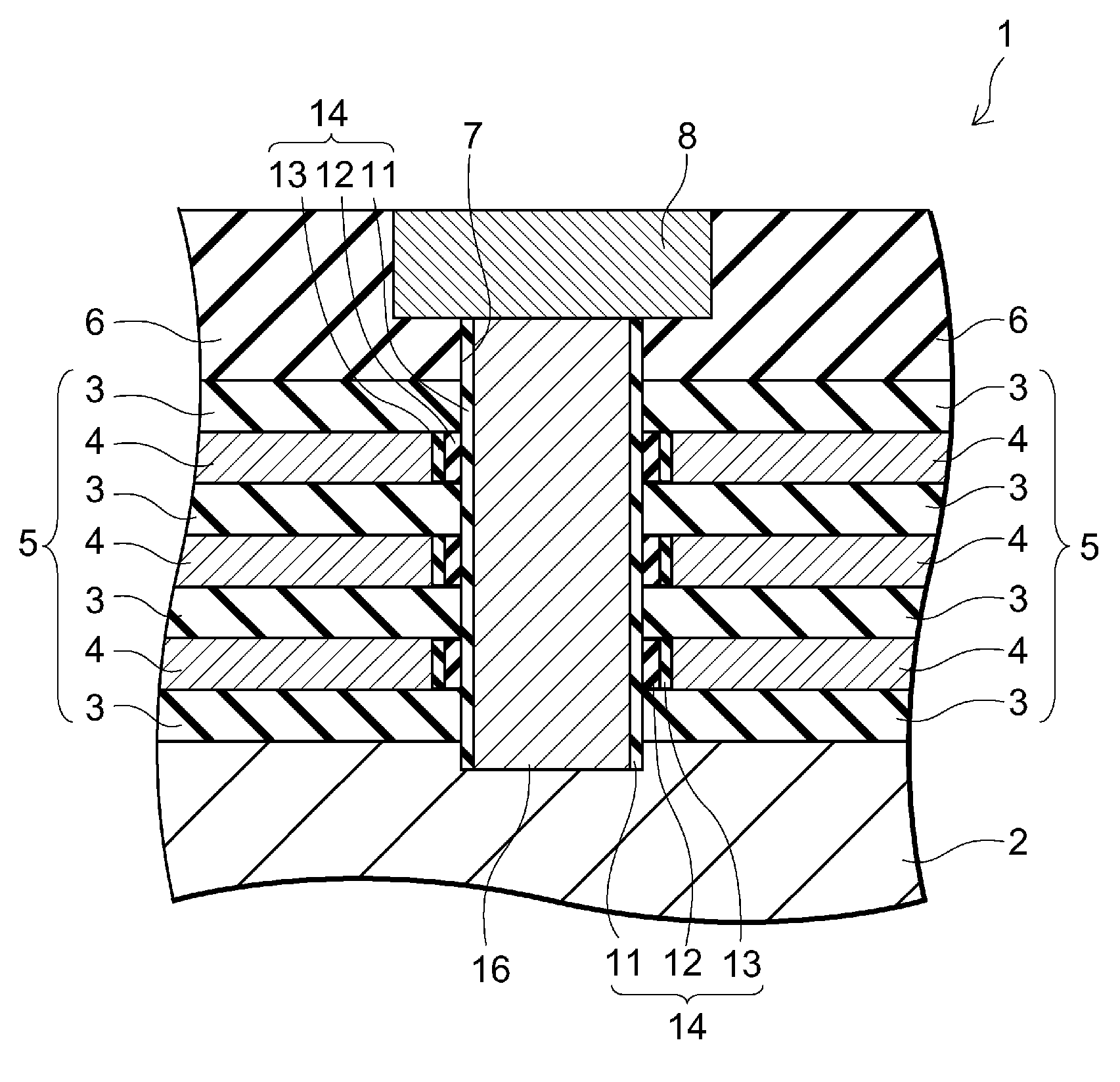
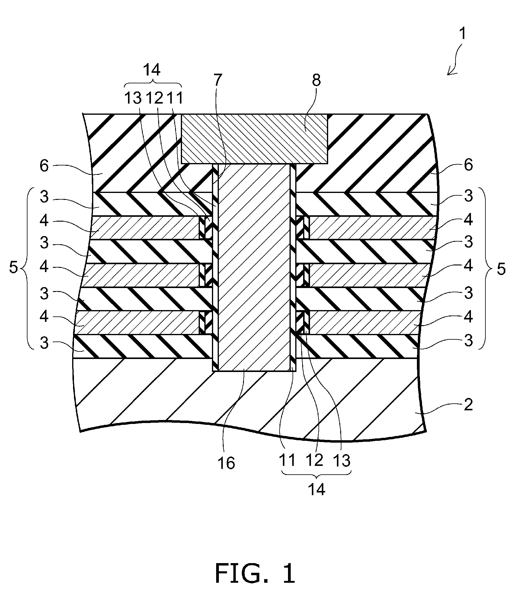
[0061]FIG. 1 is a cross-sectional view illustrating the flash memory according to this embodiment.

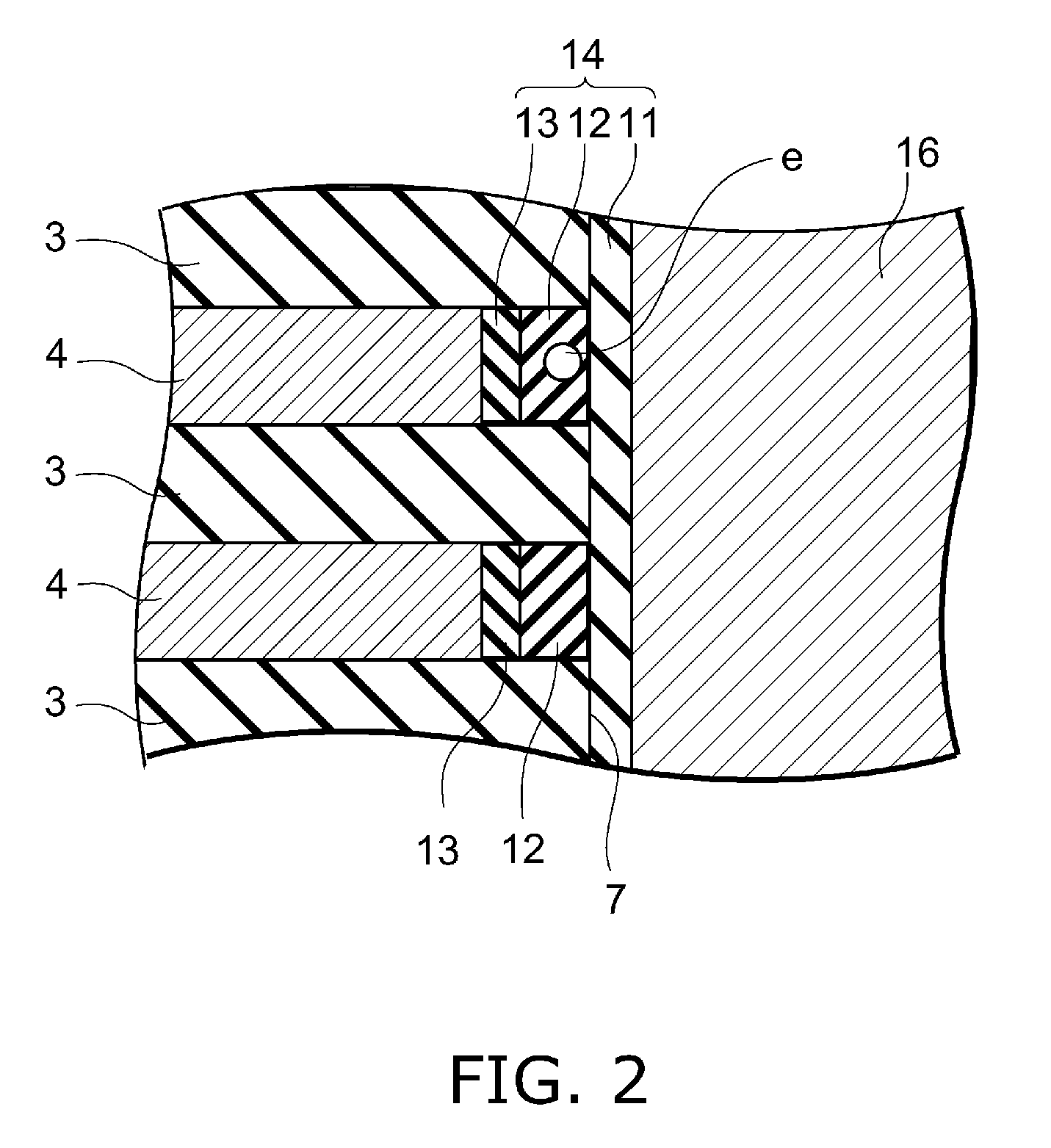
[0062]FIG. 2 is a partially enlarged view of FIG. 1.

[0063]As shown in FIG. 1, the flash memory 1 according to this embodiment includes a silicon substrate 2 illustratively made of single crystal silicon. On the silicon substrate 2, a plurality of dielectric films 3 illustratively made of silicon oxide (SiO2) and a plurality of electrode films 4 illustratively made of polycrystalline silicon are alternately laminated to form a laminated body 5. The thickness of the electrode film 4 is illustratively 50 nanometers (nm) or more. The number of electrode films 4 is illustratively 64. It is noted that for convenience of illustration, the laminated body 5 is ...

second embodiment

[0077]Next, the invention is described.

[0078]This embodiment relates to a method for manufacturing the flash memory according to the above first embodiment.

[0079]FIGS. 5A-5C and 6A-6C are process cross-sectional views illustrating the method for manufacturing a flash memory according to this embodiment.

[0080]First, as shown in FIG. 5A, a silicon substrate 2 is prepared. Then, a dielectric film 3 is formed by depositing silicon oxide on the silicon substrate 2 illustratively by CVD (chemical vapor deposition). Next, an electrode film 4 is formed by depositing polycrystalline silicon. Subsequently, likewise, dielectric films 3 and electrode films 4 are alternately deposited. Here, the thickness of the electrode film 4 is illustratively 50 nanometers or more. Thus, a laminated body 5 is formed in which a plurality of dielectric films and electrode films are alternately laminated. Subsequently, an upper dielectric film 6 is formed on the laminated body 5.

[0081]Next, as shown in FIG. 5B,...

third embodiment

[0090]Next, the invention is described.

[0091]This embodiment is an example in which the charge layer is formed from a silicon-containing metal oxide.

[0092]FIG. 7 is a cross-sectional view illustrating the flash memory according to this embodiment.

[0093]As shown in FIG. 7, the flash memory 31 according to this embodiment is different from the flash memory 1 according to the above first embodiment (see FIG. 1) in that the charge layer 12 made of silicon nitride (see FIG. 1) is replaced by a charge layer 32 made of a silicon-containing metal oxide. The charge layer 32 is illustratively formed from a material made by silicidation and oxidation of a metal such as hafnium (Hf), zirconium (Zr), tantalum (Ta), titanium (Ti), or tungsten (W). In the flash memory 31, like the above first embodiment, the charge layer 32 is split for each electrode film 4. The configuration, operation, and effect of the flash memory according to this embodiment other than the foregoing are the same as those of ...


PUM


Abstract

A laminated body is formed by alternately laminating a plurality of dielectric films and electrode films on a silicon substrate. Next, a through hole extending in the lamination direction is formed in the laminated body. Next, a selective nitridation process is performed to selectively form a charge layer made of silicon nitride in a region of an inner surface of the through hole corresponding to the electrode film. Next, a high-pressure oxidation process is performed to form a block layer made of silicon oxide between the charge layer and the electrode film. Next, a tunnel layer made of silicon oxide is formed on an inner side surface of the through hole. Thus, a flash memory can be manufactured in which the charge layer is split for each electrode film.

Description

TECHNICAL FIELD[0001]This invention relates to a nonvolatile semiconductor memory device and a method for manufacturing the same, and more particularly to a nonvolatile semiconductor memory device including a plurality of dielectric films and electrode films alternately laminated on a substrate, and a method for manufacturing the same.BACKGROUND ART[0002]Recently, to increase the density of flash memory, a technique for multilayering cells has been developed. In this technique, dielectric films and electrode films are alternately laminated on a substrate, and then collectively provided with a through hole. A charge layer for retaining charge is formed on the inner surface of this through hole, and a columnar electrode is buried inside the through hole. Thus, a flash memory with cell transistors laminated in a three-dimensional manner can be fabricated (see, e.g., Patent Citation 1).[0003]However, the flash memory thus fabricated has the problem of low reliability in retaining data f...

Claims


Application Information

Patent Timeline
IPC IPC(8): H01L27/115H01L21/8247H01L29/792H01L29/788
CPCH01L27/115H01L27/11556H01L29/7926H01L29/66833H01L29/792H01L27/11568H10B41/27H10B43/30H10B69/00H01L21/823487
Inventor KUNIYA, TAKUJIKOMORI, YOSUKEKATSUMATA, RYOTAFUKUZUMI, YOSHIAKIKITO, MASARUKIDOH, MASARUTANAKA, HIROYASUISHIDUKI, MEGUMIAOCHI, HIDEAKI
Owner KIOXIA CORP
Why Eureka
Try Eureka