Method of Fabricating Upgraded Metallurgical Grade Silicon by External Gettering Procedure

a technology of metallurgical grade silicon and gettering method, which is applied in the direction of semiconductor/solid-state device manufacturing, basic electric elements, electric apparatus, etc., can solve the problems of not providing environmental protection, no method is announced for fabricating umg-si having a purity ratio greater than 4n, and not being suitable for solar cells. , to achieve the effect of reducing the concentration of impurities

Inactive Publication Date: 2010-11-04
INST NUCLEAR ENERGY RES ROCAEC
View PDF5 Cites 30 Cited by
  • Summary
  • Abstract
  • Description
  • Claims
  • Application Information

AI Technical Summary

Benefits of technology

[0010]The main purpose of the present invention is to fabricate upgraded metallurgical grade silicon (UMG-Si) having a purity ratio between 4N and 6N by greatly reducing impurities concentration below a depth of a surface of a UMG-Si substrate.

Problems solved by technology

Between them, the internal gettering methods are not fit for solar cells.
However, the above methods are chemical methods producing chemical wastes and thus do not provide environmental protection.
In addition, no method is announced for fabricating UMG-Si having a purity ratio greater than 4N.

Method used


Image

  • Method of Fabricating Upgraded Metallurgical Grade Silicon by External Gettering Procedure
  • Method of Fabricating Upgraded Metallurgical Grade Silicon by External Gettering Procedure
  • Method of Fabricating Upgraded Metallurgical Grade Silicon by External Gettering Procedure

Examples


Embodiment Construction

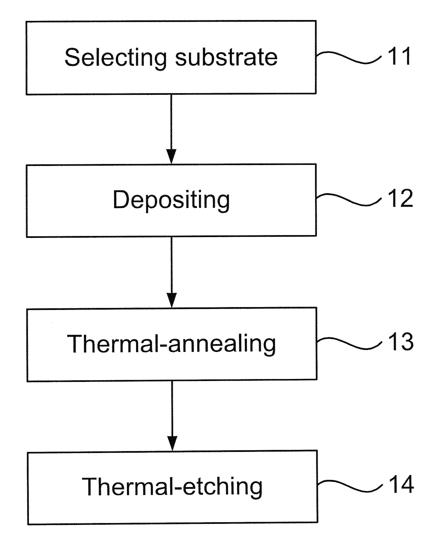
[0019]The following description of the preferred embodiment is provided to understand the features and the structures of the present invention.

[0020]Please refer to FIG. 1 until FIG. 5, which are a flow view and structural views showing the preferred embodiment according to the present invention. As shown in the figures, the present invention is a method of fabricating upgraded metallurgical grade silicon (UMG-Si) by an external gettering procedure, comprising the following steps:

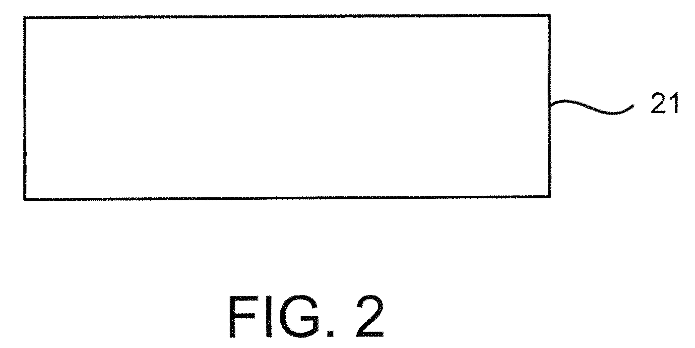
[0021](a) Selecting substrate 11: In FIG. 2, a silicon substrate is selected, where the silicon substrate is a UMG-Si substrate 21 having a purity ratio greater than 4N.

[0022](b) Depositing 12: In FIG. 3, a hydrogen-riched amorphous silicon (a-Si:H) film 22 is applied on a surface of the UMG-Si substrate 21 through physical vapor deposition (PVD) or chemical vapor deposition (CVD).

[0023](c) Thermal-annealing 13: In FIG. 4, the UMG-Si substrate 21 applied with the a-Si:H film 22 is processed through thermal-...


PUM

PropertyMeasurementUnit
thicknessaaaaaaaaaa
thicknessaaaaaaaaaa
temperatureaaaaaaaaaa

Abstract

Upgraded metallurgical grade silicon (UMG-Si) is fabricated by a ‘green’ (environmental protected) external gettering procedure. Impurities concentration of the fabricated UMG-Si is reduced for 100 times than its source material. The UMG-Si obtained has a purity ratio reaching 4N to 6N. Thus, substrates made of the UMG-Si can be used in solar cells and related photoelectrical applications.

Description

FIELD OF THE INVENTION[0001]The present invention relates to fabricating upgraded metallurgical grade silicon (UMG-Si); more particularly, relates to UMG-Si having a purity ratio between 4N and 6N by greatly reducing impurities concentration below a depth of a surface of a UMG-Si substrate.DESCRIPTION OF THE RELATED ARTS[0002]Two kinds of methods are used to remove impurities of a semiconductor material. One is internal gettering methods; and the other is external gettering methods. Between them, the internal gettering methods are not fit for solar cells.[0003]There are four external gettering methods:[0004](a) High temperature diffusion is used to directly diffuse atoms of aluminum, phosphorus, etc into the semiconductor material to form metal oxide for trapping the metal impurities.[0005](b) Mechanical-, laser- or ion-implantation is used to obtain lattice strain on surface of the semiconductor material for forming sinks of impurities.[0006](c) A thin film is applied on the semico...

Claims


Application Information

Patent Timeline
Patent Type & Authority Applications(United States)
IPC IPC(8): H01L21/322
CPCH01L21/3221
Inventor YANG, TSUN-NENG
Owner INST NUCLEAR ENERGY RES ROCAEC
Why Eureka
Try Eureka