Target object processing system and method of controlling the same
- Summary
- Abstract
- Description
- Claims
- Application Information
AI Technical Summary
Benefits of technology
Problems solved by technology
Method used
Image
Examples
Embodiment Construction
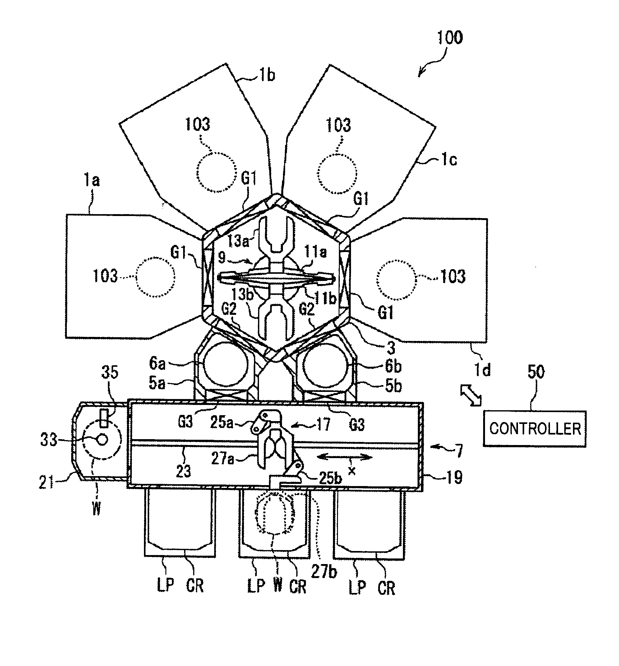
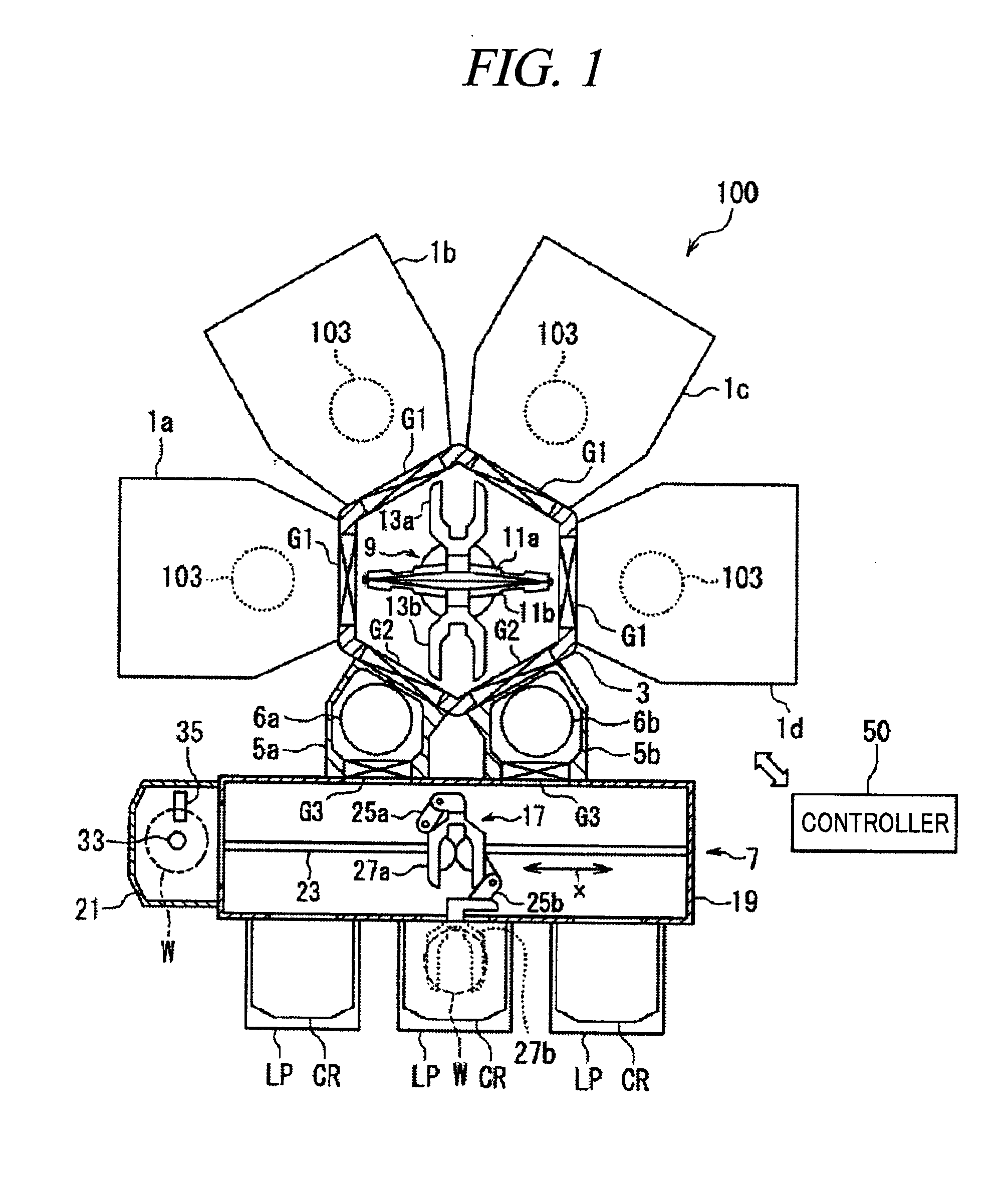
[0042]Hereinafter, embodiments of the present invention will be described. First of all, a substrate processing system in accordance with an embodiment of the present invention will be explained with reference to FIG. 1. FIG. 1 shows a schematic configuration of a substrate processing system 100 configured to perform various kinds of processes such as a film forming process or an etching process on, e.g., a semiconductor wafer W (hereinafter, simply referred to as “wafer”) as a substrate. This substrate processing system 100 is configured as a multi-chamber cluster tool.
[0043]The substrate processing system 100 includes four processing chambers 1a, 1b, 1c, and 1d configured to perform various kinds of processes on the wafer W; a vacuum transfer chamber 3 connected to each of these processing chambers 1a to 1d via each gate valve G1; two load lock chambers 5a and 5b each connected to the vacuum transfer chamber 3 via each gate valve G2; and a loader unit 7 connected to each of these ...
PUM
| Property | Measurement | Unit |
|---|---|---|
| Semiconductor properties | aaaaa | aaaaa |
Abstract
Description
Claims
Application Information


