Phase Change Memory Cells Having Vertical Channel Access Transistor and Memory Plane

Active Publication Date: 2010-11-25
MACRONIX INT CO LTD +1
View PDF99 Cites 33 Cited by
  • Summary
  • Abstract
  • Description
  • Claims
  • Application Information

AI Technical Summary

Benefits of technology

[0010]A memory device as described herein includes a plurality of bit lines and a plurality of word lines overlying the plurality of bit lines. The device includes a plurality of field effect transistors. Field effect transistors in the plurality of field effect transistors are arranged vertically, comprising a first terminal acting electrically coupled to a corresponding bit line the plurality of bit lines, a second terminal overlying the first terminal, and a channel region separating the first a

Problems solved by technology

However, reducing the size of the phase change element by etching can result in damage to the phase change material due to non-uniform reactivity with the etchants which can cause the formation of voids, compositional and bonding variations, and the formation of nonvolatile by-products.
This damage can result in variations in shape and uniformity of the phase change elements across an array of memory cells, resulting in electrical and mechanical performance issues for the cell.
However, traditional field effect transistor access devices are horizontal structures having a horizontally oriented gate overlying a horizontally oriented channel regi

Method used


Image

  • Phase Change Memory Cells Having Vertical Channel Access Transistor and Memory Plane
  • Phase Change Memory Cells Having Vertical Channel Access Transistor and Memory Plane
  • Phase Change Memory Cells Having Vertical Channel Access Transistor and Memory Plane

Examples


Example

[0023]The following description of the disclosure will typically be with reference to specific structural embodiments and methods. It is to be understood that there is no intention to limit the disclosure to the specifically disclosed embodiments and methods, but that the disclosure may be practiced using other features, elements, methods and embodiments. Preferred embodiments are described to illustrate the present disclosure, not to limit its scope, which is defined by the claims. Those of ordinary skill in the art will recognize a variety of equivalent variations on the description that follows. Like elements in various embodiments are commonly referred to with like reference numerals.

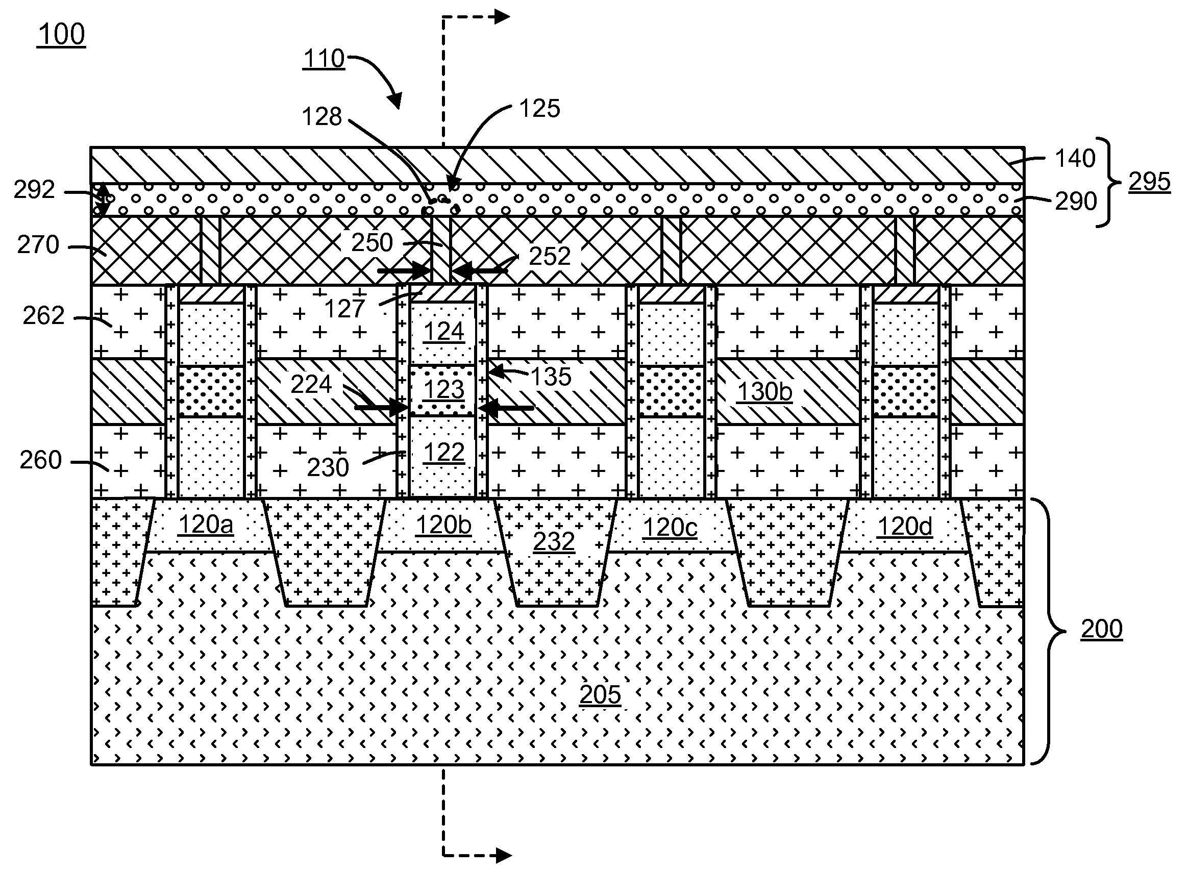
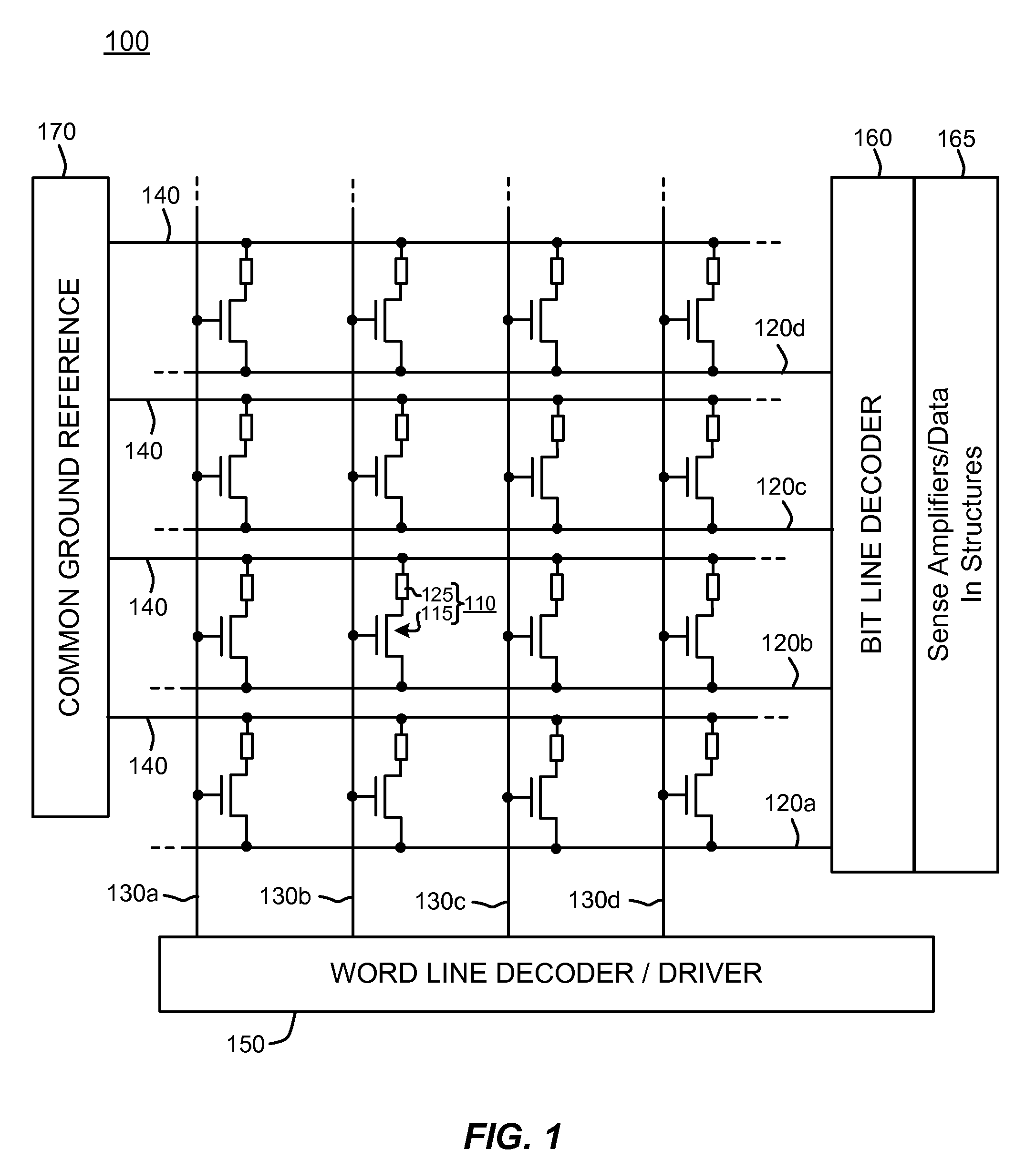
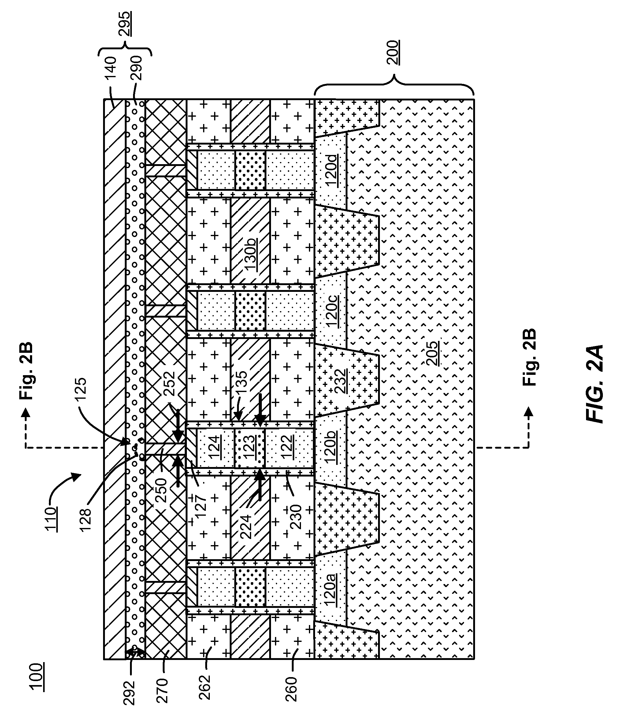
[0024]FIG. 1 illustrates a schematic diagram of a portion of a memory cell array 100 implemented using memory cells having field effect transistors with vertical channels and memory elements comprising programmable resistance material of a memory plane as described herein.

[0025]As shown in the schem...


PUM


Abstract

Memory devices are described along with methods for manufacturing. A memory device as described herein comprises a plurality of word lines overlying a plurality of bit lines, and a plurality of field effect transistors. Field effect transistors in the plurality of field effect transistors comprises a first terminal electrically coupled to a corresponding bit line in the plurality of bit lines, a second terminal overlying the first terminal, and a channel region separating the first and second terminals and adjacent a corresponding word line in the plurality of word lines. The corresponding word line acts as the gate of the field effect transistor. A dielectric separates the corresponding word line from the channel region. A memory plane comprises programmable resistance memory material electrically coupled to respective second terminals of the field effect transistors, and conductive material on the programmable resistance memory material and coupled to a common voltage.

Description

BACKGROUND OF THE INVENTION[0001]1. Field of the Invention[0002]The present invention relates to high density memory devices based on phase change memory materials, including chalcogenide based materials and on other programmable resistance materials, and methods for manufacturing such devices.[0003]2. Description of Related Art[0004]Phase change based memory materials, like chalcogenide based materials and similar materials, can be caused to change phase between an amorphous state and a crystalline state by application of electrical current at levels suitable for implementation in integrated circuits. The generally amorphous state is characterized by higher electrical resistivity than the generally crystalline state, which can be readily sensed to indicate data. These properties have generated interest in using programmable resistance material to form nonvolatile memory circuits, which can be read and written with random access.[0005]The change from the amorphous to the crystalline...

Claims


Application Information

Patent Timeline
IPC IPC(8): H01L47/00H01L21/00
CPCG11C13/0004H01L45/1683H01L27/2454H01L27/2463H01L45/04H01L45/06H01L45/085H01L45/1233H01L45/142H01L45/144H01L45/146H01L45/147H01L45/1625H01L45/1641H01L45/1675H01L27/101
Inventor LUNG, HSIANG-LANLAM, CHUNG H.LEE, MING-HSIURAJENDRAN, BIPIN
Owner MACRONIX INT CO LTD
Why Eureka
Try Eureka