Nonvolatile Memory Device and Method of Manufacturing the Same

a non-volatile memory and manufacturing method technology, applied in semiconductor devices, semiconductor/solid-state device details, electrical devices, etc., can solve the problems of source or drain loss, error generation in the operation of non-volatile memory devices, etc., to improve the occurrence of errors in the operation.

Inactive Publication Date: 2010-11-25
SK HYNIX INC
View PDF5 Cites 4 Cited by
  • Summary
  • Abstract
  • Description
  • Claims
  • Application Information

AI Technical Summary

Benefits of technology

[0007]An exemplary embodiment relates to a nonvolatile memory device and a method of manufacturing the same, which are capable of improving the oc

Problems solved by technology

However, the source or the drain can be lost in a process of manufacturing a nonvolatile memory device.
Accordingly, there is a problem in th

Method used


Image

  • Nonvolatile Memory Device and Method of Manufacturing the Same
  • Nonvolatile Memory Device and Method of Manufacturing the Same
  • Nonvolatile Memory Device and Method of Manufacturing the Same

Examples


Embodiment Construction

[0022]Hereinafter, exemplary embodiments of the disclosure are described in detail with reference to the accompanying drawings. The drawing figures are provided to allow those having ordinary skill in the art to understand the scope of the embodiments of the disclosure.

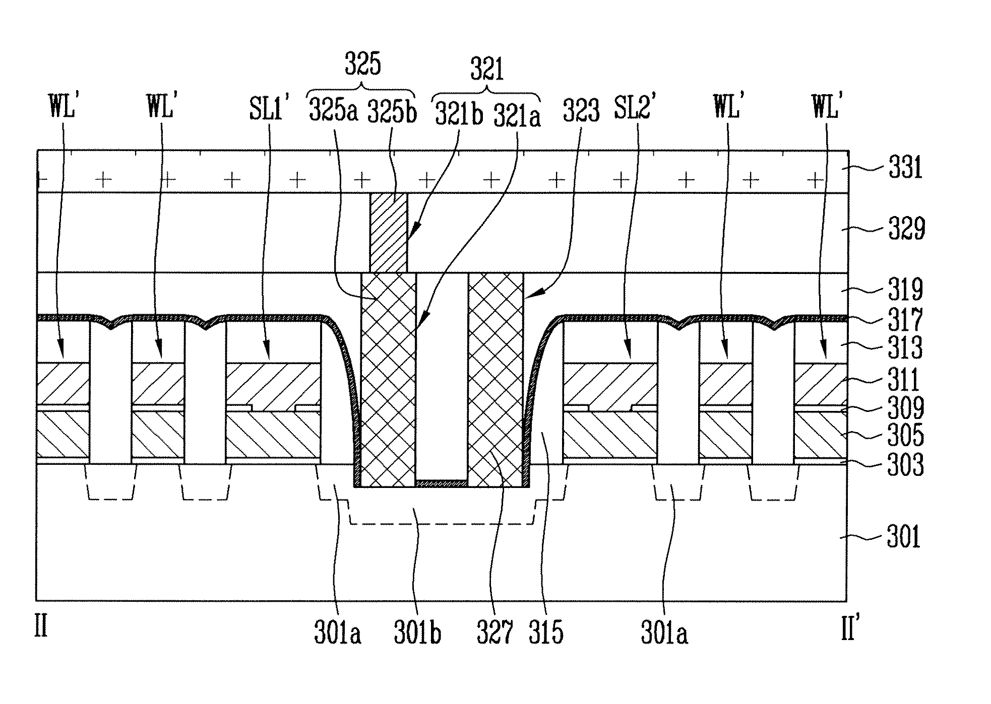
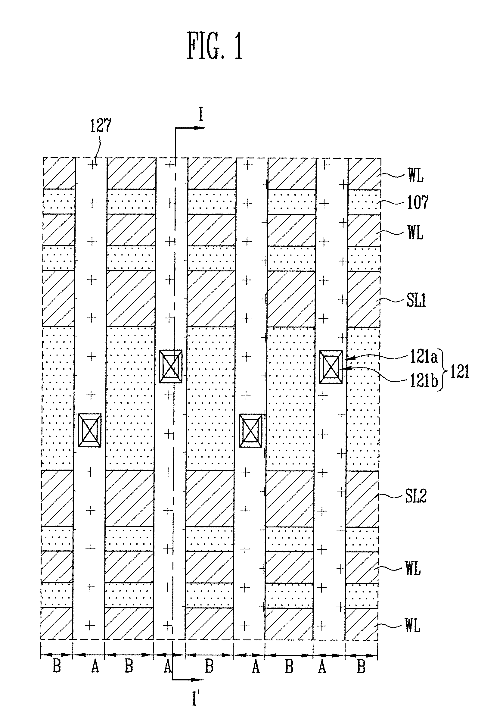
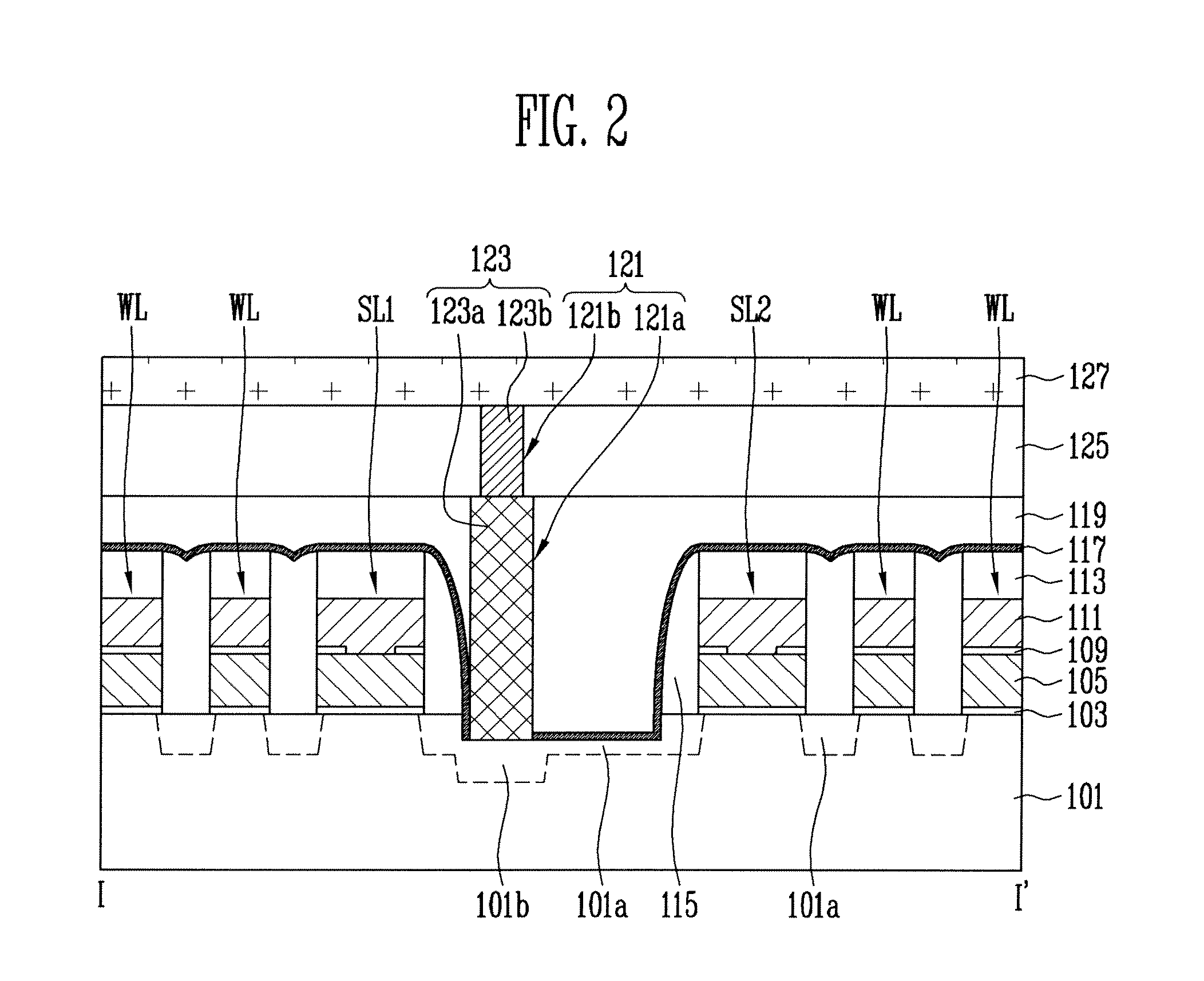
[0023]FIG. 1 is a layout diagram schematically showing part of a memory cell array of a nonvolatile memory device. FIG. 2 is a cross-sectional view of the memory cell array taken along line I-I′ shown in FIG. 1. The nonvolatile memory devices shown in FIGS. 1 and 2 are NAND flash memory devices.

[0024]Referring to FIGS. 1 and 2, the gate of the NAND flash memory device is formed over a semiconductor substrate 101 with a gate insulating layer 103 interposed between the gate and the semiconductor substrate 101. The semiconductor substrate 101 includes active regions A and isolation regions B, which are parallel to each other and alternately arranged with respect to each other. An isolation layer 107 is formed in the isol...


PUM


Abstract

A nonvolatile memory device comprises a semiconductor substrate comprising alternating, parallel active regions and isolation regions; first and second selection lines intersecting the active regions and the isolation regions; first junctions formed in the active regions between the first and second selection lines; spacers formed on sidewalls of the first and second selection lines; second junctions deeper than the first junctions formed in the first junctions, respectively; contact plugs coupled to one side of the respective second junctions; and dummy plugs coupled second sides of the respective second junctions.

Description

CROSS-REFERENCE TO RELATED APPLICATION[0001]Priority to Korean patent application number 10-2009-0045401 filed on May 25, 2009, the entire disclosure of which is incorporated by reference herein, is claimed.BACKGROUND[0002]Exemplary embodiments relate to a nonvolatile memory device and a method of manufacturing the same and, more particularly, to a nonvolatile memory device and a method of manufacturing the same, which are capable of improving passage of current from a signal line to a string structure.[0003]NAND flash memory devices, a type of nonvolatile memory device facilitating higher capacity and higher degree of integration, have been actively developed. The memory cell array of the NAND flash memory device includes string structures arranged in a matrix form. Each of the string structures includes a drain select transistor having a drain coupled to a bit line, a source select transistor having a source coupled to a common source line, and a number of memory cells coupled in ...

Claims


Application Information

Patent Timeline
IPC IPC(8): H01L23/48H01L21/768
CPCH01L21/76816H01L21/76897H01L27/11524H01L29/66659H01L29/66636H10B41/35H01L21/28141H10B41/40H10B41/30
Inventor PARK, SUN MI
Owner SK HYNIX INC
Why Eureka
Try Eureka