Organic electroluminescent device

a technology of electroluminescent devices and organic materials, applied in the direction of organic semiconductor devices, discharge tube luminescnet screens, pyrene dyes, etc., can solve problems such as efficiency improvement, and achieve the effect of improving efficiency and lifetime of fluorescent devices, and improving efficiency of fluorescent devices

Inactive Publication Date: 2010-11-25
IDEMITSU KOSAN CO LTD
View PDF12 Cites 64 Cited by
  • Summary
  • Abstract
  • Description
  • Claims
  • Application Information

AI Technical Summary

Benefits of technology

[0019]The inventors noticed a phenomenon stated in Non-Patent Document 1, i.e. a phenomenon in which singlet excitons are generated by collision and fusion of two triplet excitons (hereinafter referred to as Triplet-Triplet Fusion=TTF phenomenon), and made studies in an attempt to improve efficiency of a fluorescent device by allowing the TTF phenomenon to occur efficiently. Specifically, the inventors made studies on various combinations of a host material (hereinafter often referred to simply as a “host”) and a fluorescent dopant material (hereinafter often referred to simply as a “dopant”). As a result of the studies, the inventors have found that when the triplet energy of a host and that of a dopant satisfies a specific relationship, and a material having large triplet energy is used in a layer which is adjacent to the interface on the cathode side of an emitting layer (referred to as a “blocking layer” in the invention), triplet excitons are confined within the emitting layer to allow the TTF phenomenon to occur efficiently, whereby improvement in efficiency and lifetime of a fluorescent device can be realized.

Problems solved by technology

In a phosphorescent device, efficient confinement of triplet excitons within an emitting layer does not necessarily result in improvement in efficiency.

Method used


Image

  • Organic electroluminescent device
  • Organic electroluminescent device
  • Organic electroluminescent device

Examples


first embodiment

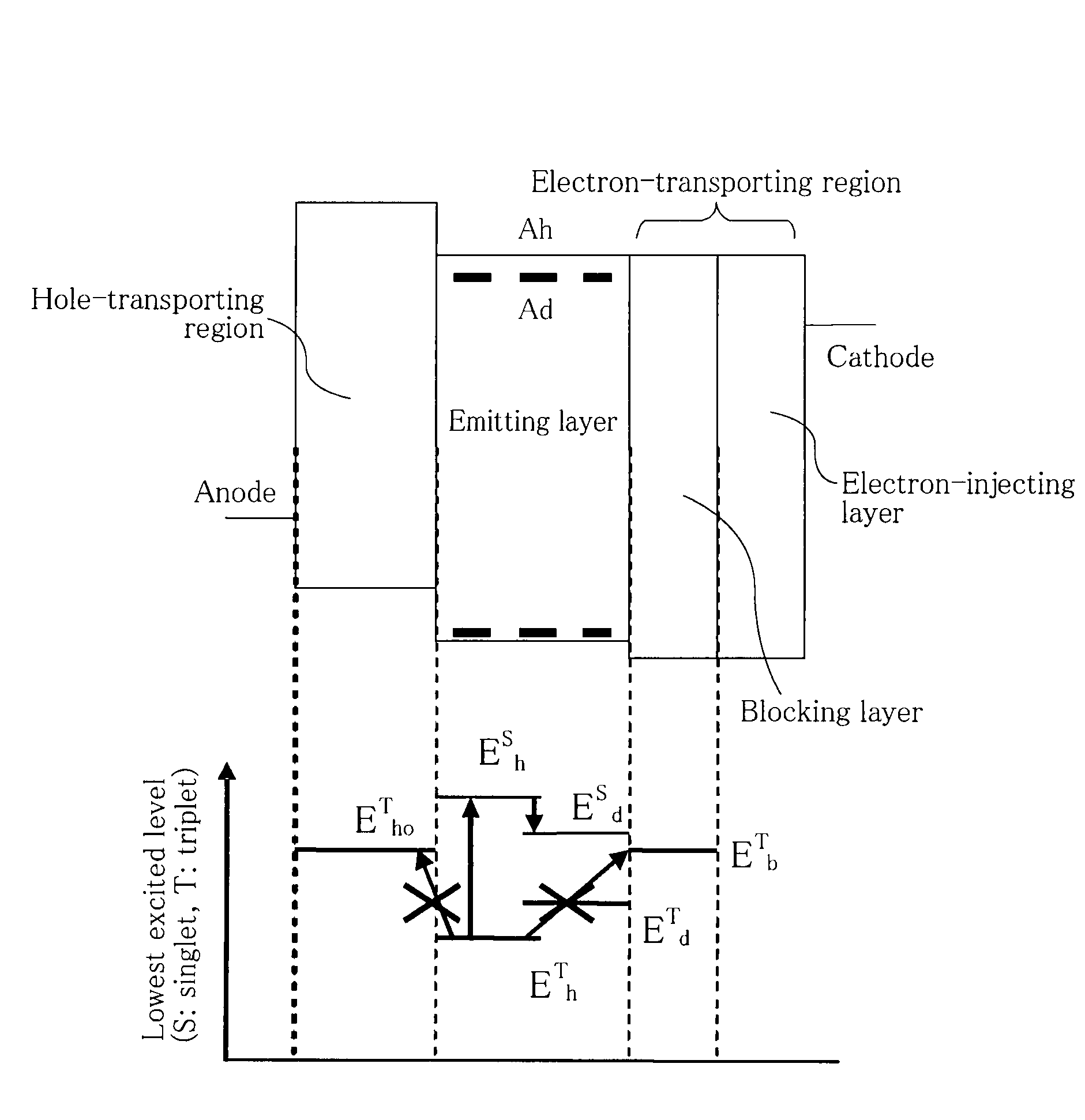
[0056]The invention utilizes the TTF phenomenon. First, an explanation is made of the TTF phenomenon.

[0057]Holes and electrons injected from an anode and a cathode are recombined with an emitting layer to generate excitons. As for the spin state, as is conventionally known, singlet excitons account for 25% and triplet excitons account for 75%. In a conventionally known fluorescent device, light is emitted when singlet excitons of 25% are relaxed to the ground state. The remaining triplet excitons of 75% are returned to the ground state without emitting light through a thermal deactivation process. Accordingly, the theoretical limit value of the internal quantum efficiency of a conventional fluorescent device is believed to be 25%.

[0058]The behavior of triplet excitons generated within an organic substance has been theoretically examined. According to S. M. Bachilo et al. (J. Phys. Chem. A, 104, 7711 (2000)), assuming that high-order excitons such as quintet excitons are quickly retu...

second embodiment

[0131]When the triplet energies of the host, the dopant and the material for the blocking layer satisfy the specified relationship, the ratio of the luminous intensity derived from TTF can be 30% or more of the total emission. As a result, a high efficiency which cannot be realized by conventional fluorescent devices can be attained.

[0132]The ratio of luminous intensity derived from TTF can be measured by the transient EL method. The transient EL method is a technique for measuring a decay behavior (transient properties) of EL emission after removal of a DC voltage applied to a device. EL luminous intensity is classified into luminous components from singlet excitons which are generated by the first recombination and luminous components from singlet excitons generated through the TTF phenomenon. The lifetime of a singlet exciton is very short, i.e. on the nanosecond order. Therefore, this emission decays quickly after removal of a DC voltage. On the other hand, the TTF phenomenon is...

third embodiment

[0138]The device of the invention may have a tandem device configuration in which at least two emitting layers are provided. An intermediate layer is provided between the two emitting layers. Of the two emitting layers, at least one is a fluorescent emitting layer, which satisfies the above-mentioned requirements. Specific examples of device configuration are given below.

[0139]Anode / fluorescent emitting layer / intermediate layer / fluorescent emitting layer / electron-transporting region / cathode

[0140]Anode / fluorescent emitting layer / electron-transporting region / intermediate layer / fluorescent emitting layer / cathode

[0141]Anode / fluorescent emitting layer / electron-transporting region / intermediate layer / fluorescent emitting layer / electron-transporting region / cathode

[0142]Anode / phosphorescent emitting layer / intermediate layer / fluorescent emitting layer / electron-transporting region / cathode

[0143]Anode / fluorescent emitting layer / electron-transporting region / intermediate layer / phosphorescent emitt...


PUM


Abstract

An organic electroluminescence device containing an anode, an emitting layer, a blocking layer, an electron-injecting layer and a cathode in sequential order; wherein the emitting layer contains a host and a dopant which gives fluorescent emission of which the main peak wavelength is 550 nm or less; the affinity Ad of the dopant is smaller than the affinity Ah of the host; the triplet energy ETd of the dopant is larger than the triplet energy ETh of the host; the triplet energy ETb of the blocking layer is larger than ETh; the affinity Ab of the blocking layer and the affinity Ae of the electron-injecting layer satisfies Ae−Ab≦0.2 eV; and the electron mobility of the material constituting the blocking layer is 10−6 cm2/Vs or more in an electric field intensity of 0.04 to 0.5 MV/cm.

Description

TECHNICAL FIELD[0001]The invention relates to an organic electroluminescence (EL) device, particularly, to a highly efficient organic EL device.BACKGROUND ART[0002]An organic EL device can be classified into two types, i.e. a fluorescent EL device and a phosphorescent EL device according to its emission principle. When a voltage is applied to an organic EL device, holes are injected from an anode, and electrons are injected from a cathode, and holes and electrons recombine in an emitting layer to form excitons. According to the electron spin statistics theory, singlet excitons and triplet excitons are formed at an amount ratio of 25%:75%. In a fluorescent EL device which uses emission caused by singlet excitons, the limited value of the internal quantum efficiency is believed to be 25%. Technology for prolonging the lifetime of a fluorescent EL device utilizing a fluorescent material has been recently improved. This technology is being applied to a full-color display of portable pho...

Claims


Application Information

Patent Timeline
Patent Type & Authority Applications(United States)
IPC IPC(8): H01J1/63
CPCH01L51/005H01L51/0054H01L51/0058H01L51/006H01L51/5016C09B69/008H05B33/10H05B33/14C09B57/00C09B57/001C09B57/008H01L2251/552H10K85/60H10K85/622H10K85/626H10K85/633H10K50/11H10K2101/10H10K2101/30H10K85/615
Inventor KUMA, HITOSHIKAWAMURA, YUICHIROJINDE, YUKITOSHIOGIWARA, TOSHINARIHOSOKAWA, CHISHIO
Owner IDEMITSU KOSAN CO LTD
Why Eureka
Try Eureka