
Fast switching, overshoot-free, current source and method
a current source and current source technology, applied in the direction of electric variable regulation, pulse automatic control, instruments, etc., can solve the problems of high silicon area consumption, high power consumption, and risk of not matching all specifications, and achieve low impedance nodes, reduce output current overshoots, and reduce the effect of overshoots
- Summary
- Abstract
- Description
- Claims
- Application Information
AI Technical Summary
Benefits of technology
Problems solved by technology
Method used
Image

Examples
Embodiment Construction
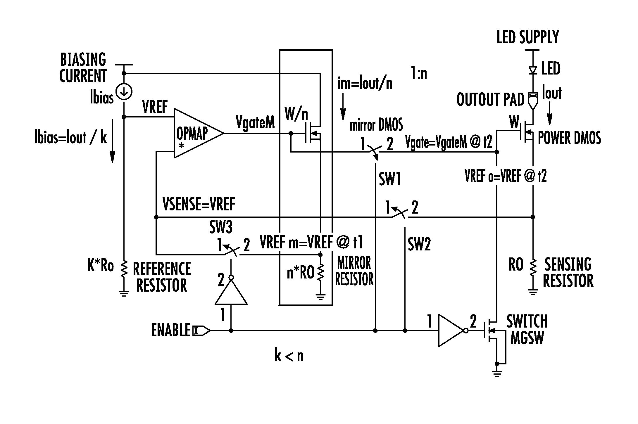
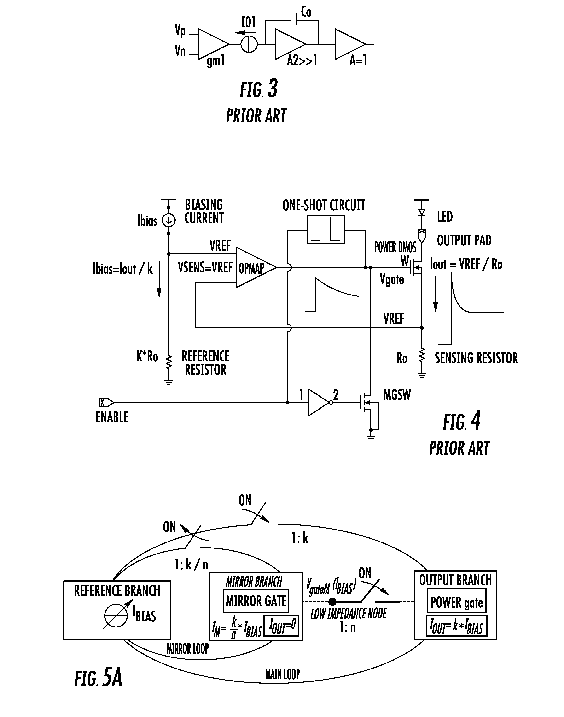
[0047]With reference to the diagram of FIG. 5a that represents the principle of functioning of the current source circuit of this disclosure, the inner replica feedback loop includes an n time scaled down replica of the power switch (e.g. a DMOS of size W / n, where W is the size of the output power DMOS) and a sensing resistor of n time greater resistance (e.g. of resistance n*R0 where R0 is the resistance of the sensing resistor of the main or reference feedback loop). At the gate of the output power element, the ideal (Thevenin equivalent) situation is represented by the equivalent circuit of FIG. 5b.
[0048]As may be immediately recognized by observing the circuits of FIGS. 5a and 5b: speed depends by the speed with which the control switches couple either the replica feedback loop (briefly designated with an added “M” notation, short for “mirror”) or the main reference feedback loop to the dedicated input of the op-amp; this dramatically shortens rise time and allows a good contro...
PUM
| Property | Measurement | Unit |
|---|---|---|
| rise time | aaaaa | aaaaa |
| current | aaaaa | aaaaa |
| voltage drop | aaaaa | aaaaa |
Abstract
Description
Claims
Application Information