Gradient Ternary or Quaternary Multiple-Gate Transistor

a multi-gate, ternary or quaternary technology, applied in the field of integrated circuit devices, can solve the problems of high leakage current of mos transistors, high band-to-band leakage current between gate and source/drain region, etc., to improve the performance of mos transistors, reduce leakage current, and improve drive current

Active Publication Date: 2010-12-02
TAIWAN SEMICON MFG CO LTD
View PDF76 Cites 115 Cited by
  • Summary
  • Abstract
  • Description
  • Claims
  • Application Information

AI Technical Summary

Benefits of technology

[0009]The advantageous features of the present invention include improved performance in MOS transis

Problems solved by technology

A challenge faced by the semiconductor industry, however, is that although the MOS transistors formed on III-V compound semiconductors or germanium have high drive currents, the leakag

Method used


Image

  • Gradient Ternary or Quaternary Multiple-Gate Transistor
  • Gradient Ternary or Quaternary Multiple-Gate Transistor
  • Gradient Ternary or Quaternary Multiple-Gate Transistor

Examples


Embodiment Construction

[0016]The making and using of the embodiments of the present invention are discussed in detail below. It should be appreciated, however, that the embodiments provide many applicable inventive concepts that can be embodied in a wide variety of specific contexts. The specific embodiments discussed are merely illustrative of specific ways to make and use the invention, and do not limit the scope of the invention.

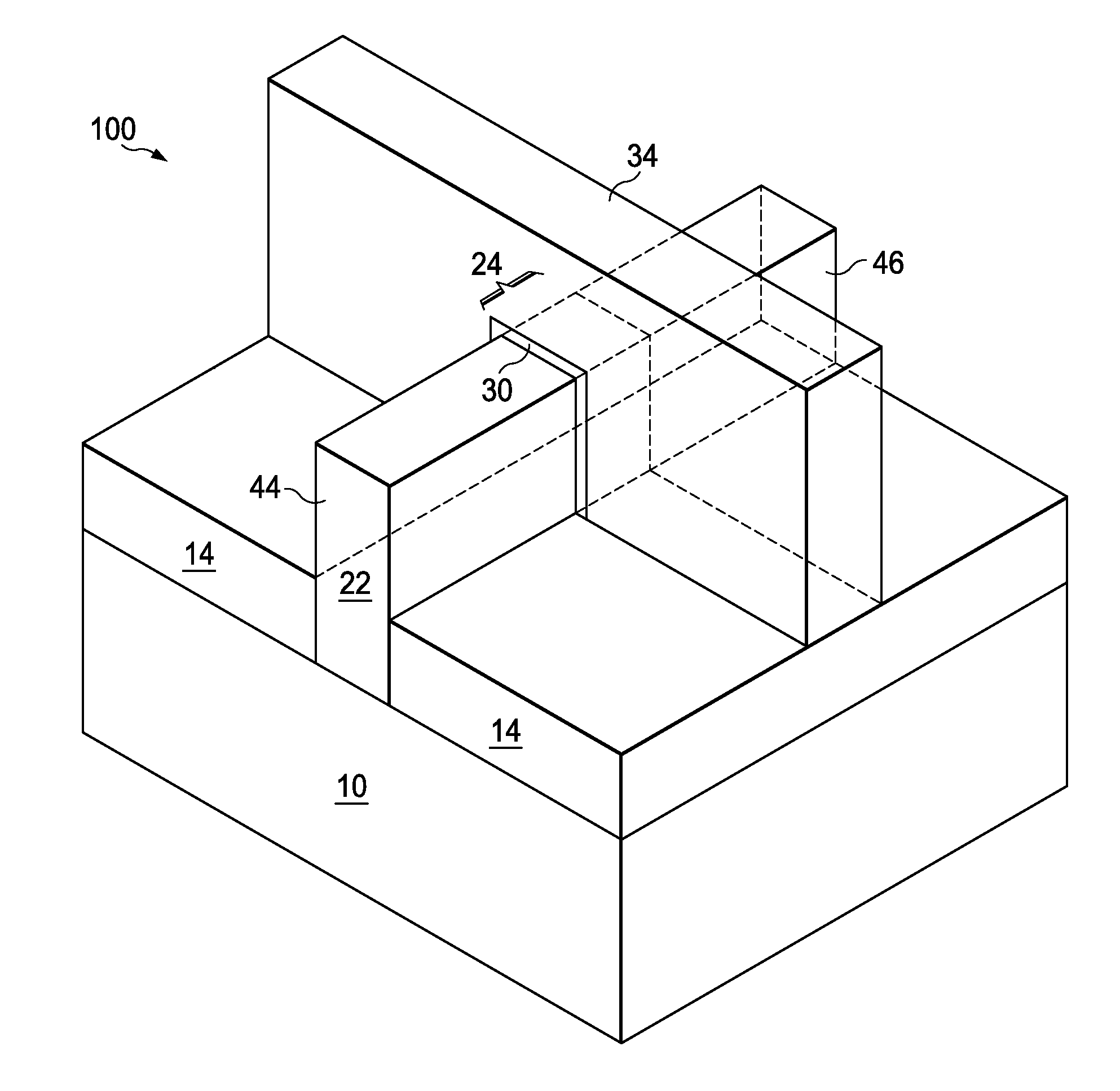
[0017]Novel fin field-effect transistors (FinFETs) and the method of forming the same are presented. The intermediate stages of manufacturing embodiments of the present invention are illustrated. The variations and the operation of the embodiments are discussed. Throughout the various views and illustrative embodiments of the present invention, like reference numbers are used to designate like elements.

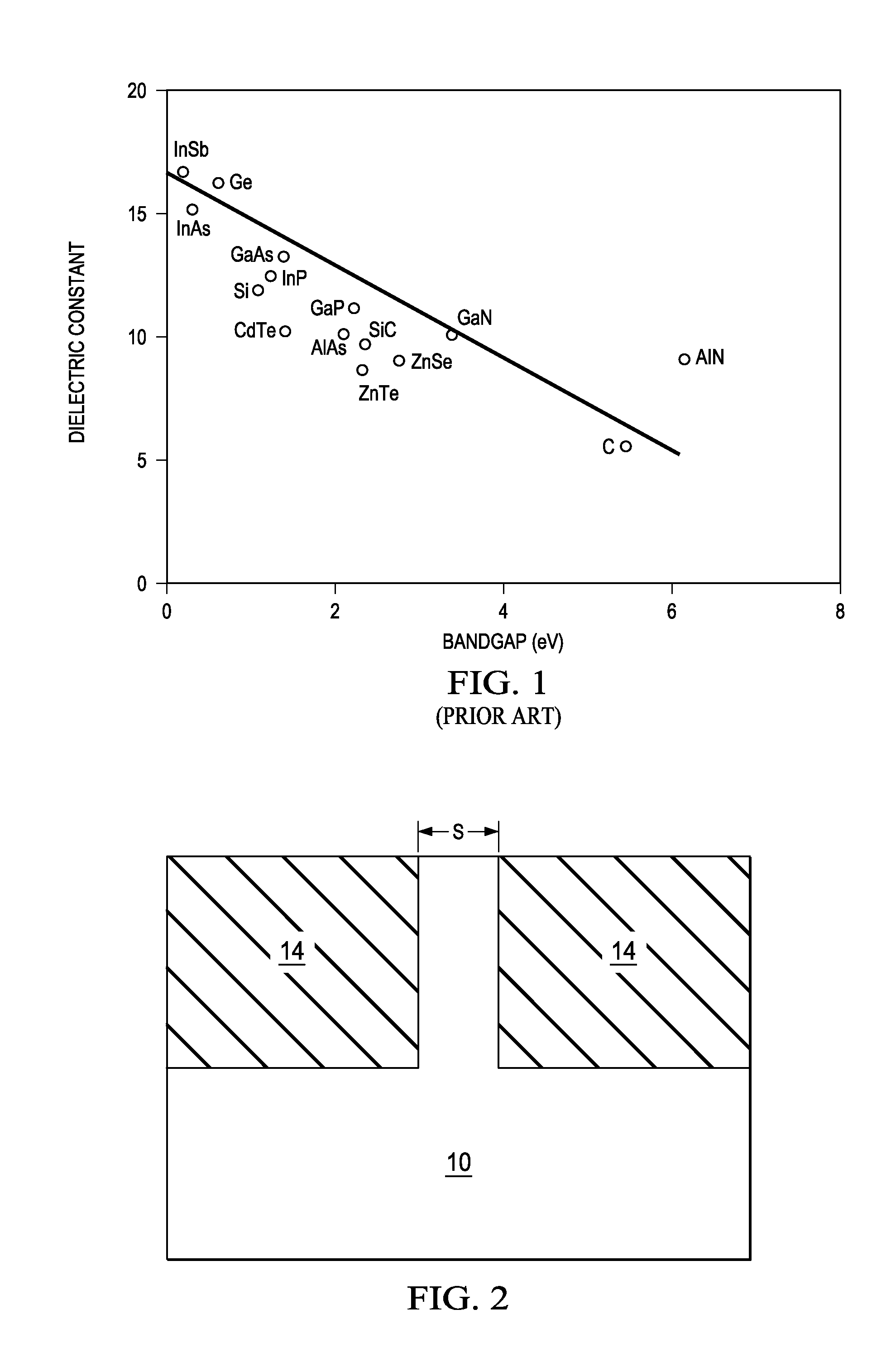
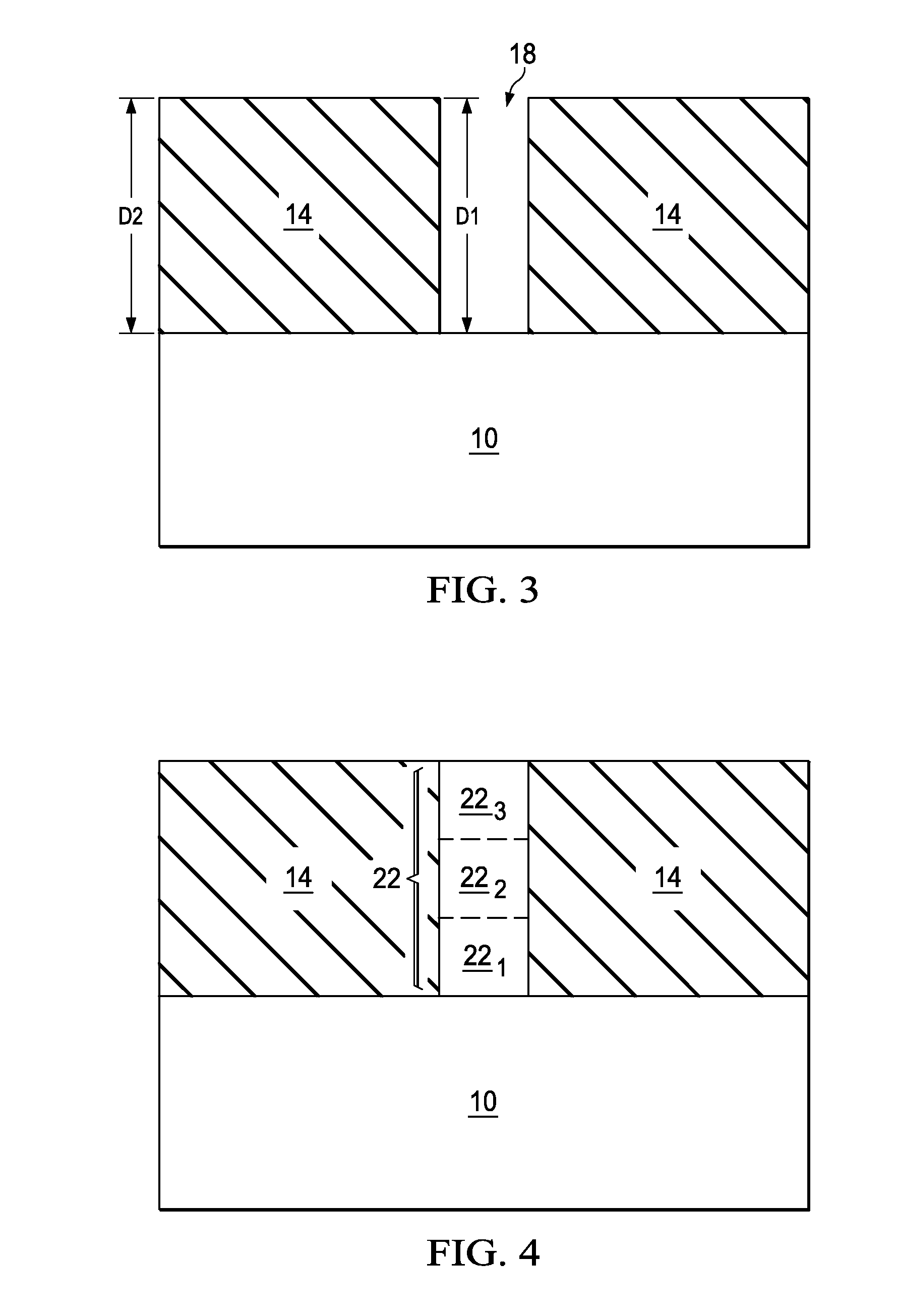
[0018]FIGS. 2 through 6 illustrate the cross-sectional views of intermediate stages in the manufacturing of a FinFET. Referring to FIG. 2, substrate 10 is provided. Substrate 10 ...


PUM


Abstract

An integrated circuit structure includes a semiconductor substrate; insulation regions over the semiconductor substrate; and an epitaxy region over the semiconductor substrate and having at least a portion in a space between the insulation regions. The epitaxy region includes a III-V compound semiconductor material. The epitaxy region also includes a lower portion and an upper portion over the lower portion. The lower portion and the semiconductor substrate have a first lattice mismatch. The upper portion and the semiconductor substrate have a second lattice mismatch different from the first lattice mismatch.

Description

[0001]This application claims the benefit of U.S. Provisional Application No. 61 / 182,550 filed on May 29, 2009, entitled “Gradient Ternary or Quaternary Multiple-Gate Transistor,” which application is hereby incorporated herein by reference.CROSS-REFERENCE TO RELATED APPLICATION[0002]This application relates to commonly-assigned U.S. Provisional Patent Application Ser. No. 61 / 165,803, filed Apr. 1, 2009, and entitled “High-Mobility Multiple-Gate Transistor with Improved On-to-Off Current Ratio,” which application is hereby incorporated herein by reference.TECHNICAL FIELD[0003]This invention relates generally to integrated circuit devices, and more particularly to fin field-effect transistors (FinFETs) and methods for forming the same.BACKGROUND[0004]The speeds of metal-oxide-semiconductor (MOS) transistors are closely related to the drive currents of the MOS transistors, which drive currents are further closely related to the mobility of charges. For example, NMOS transistors have h...

Claims


Application Information

Patent Timeline
IPC IPC(8): H01L31/0304
CPCH01L29/7851H01L29/66795
Inventor KO, CHIH-HSINWANN, CLEMENT HSINGJEN
Owner TAIWAN SEMICON MFG CO LTD
Why Eureka
Try Eureka