Profiled contact for semiconductor device

a semiconductor device and contact technology, applied in the field of contacts for devices, can solve the problems of little or no approach to use electrode shaping to achieve a higher breakdown voltage and/or eliminate direct inter-electrode breakdown, and the breakdown has not been frequent. , to achieve the effect of eliminating direct inter-electrode breakdown, high breakdown field, and high breakdown voltag

Active Publication Date: 2010-12-02
SENSOR ELECTRONICS TECH
View PDF1 Cites 5 Cited by
  • Summary
  • Abstract
  • Description
  • Claims
  • Application Information

AI Technical Summary

Benefits of technology

[0009]The inventors recognize that breakdown in the air or encapsulating material may occur before the breakdown field in the semiconductor has been reached when the device is fabricated using a semiconductor material with a high breakdown field, such as GaN. Currently, such breakdowns have not been frequent due to, for example, rough edges of the contacts typically used. As a result, little or no approaches have sought to use electrode shaping to achieve a higher breakdown voltage and / or eliminate direct inter-electrode breakdown. The inventors propose that reducing or eliminating the possibility for breakdown in the surrounding air or encapsulating material between electrodes can comprise an important solution to achieve a higher operating voltage of a device, e.g., an operating voltage close to the breakdown voltage of the bulk of the semiconductor material used to fabricate the device.

Problems solved by technology

Currently, such breakdowns have not been frequent due to, for example, rough edges of the contacts typically used.
As a result, little or no approaches have sought to use electrode shaping to achieve a higher breakdown voltage and / or eliminate direct inter-electrode breakdown.

Method used


Image

  • Profiled contact for semiconductor device
  • Profiled contact for semiconductor device
  • Profiled contact for semiconductor device

Examples


Embodiment Construction

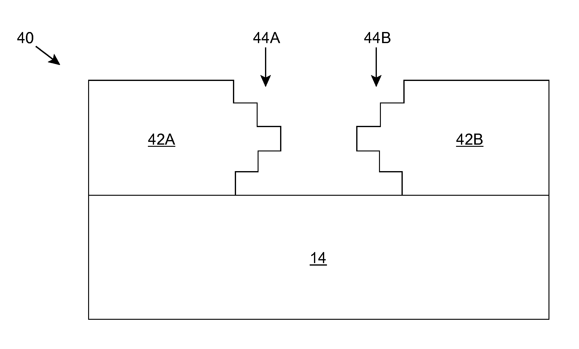
[0025]As indicated above, aspects of the invention provide a profiled contact for a device, such as a high power semiconductor device. The contact is profiled in both a direction substantially parallel to a surface of a semiconductor structure of the device and a direction substantially perpendicular to the surface of the semiconductor structure. The profiling can limit the peak electric field between two electrodes to approximately the same as the average electrical field between the electrodes, as well as limit the electric field perpendicular to the semiconductor structure both within and outside the semiconductor structure. As used herein, unless otherwise noted, the term “set” means one or more (i.e., at least one) and the phrase “any solution” means any now known or later developed solution.

[0026]Aspects of the invention provide a solution for designing one or more electrodes for a semiconductor device to reduce the electric field above the semiconductor surface (e.g., in the ...


PUM

PropertyMeasurementUnit
temperatureaaaaaaaaaa
electric fieldaaaaaaaaaa
critical electric fieldaaaaaaaaaa

Abstract

A profiled contact for a device, such as a high power semiconductor device is provided. The contact is profiled in both a direction substantially parallel to a surface of a semiconductor structure of the device and a direction substantially perpendicular to the surface of the semiconductor structure. The profiling can limit the peak electric field between two electrodes to approximately the same as the average electrical field between the electrodes, as well as limit the electric field perpendicular to the semiconductor structure both within and outside the semiconductor structure.

Description

REFERENCE TO PRIOR APPLICATIONS[0001]The current application claims the benefit of co-pending U.S. Provisional Application No. 61 / 217,531, titled “High voltage semiconductor device”, which was filed on 1 Jun. 2009, and which is hereby incorporated by reference.TECHNICAL FIELD[0002]The disclosure relates generally to contacts for devices, and more particularly, to a profiled contact for a semiconductor device, such as a high voltage semiconductor device.BACKGROUND ART[0003]High voltage operation of devices, such as semiconductor devices, has remained a focus of intense research for decades. An ability of a semiconductor device to operate at a high level of bias and signal voltage is an important characteristic defining an overall device figure of merit. When an operating voltage approaches or exceeds the breakdown voltage for a particular semiconductor material and / or device structure and layout, the device becomes inoperable due to non-recoverable damage to the semiconductor materia...

Claims


Application Information

Patent Timeline
Patent Type & Authority Applications(United States)
IPC IPC(8): H01L23/535G06F17/50H01L21/768H01L21/67
CPCH01L29/41708H01L29/42312H01L29/42308H01L29/41716H01L29/41725Y10T29/41H01L29/42304
Inventor SIMIN, GRIGORYSHUR, MICHAELGASKA, REMIGIJUS
Owner SENSOR ELECTRONICS TECH
Why Eureka
Try Eureka