
Nanoimprint resist, nanoimprint mold and nanoimprint lithography

a technology of nanoimprinting and resisting nanostructures, applied in photomechanical devices, instruments, manufacturing tools, etc., can solve problems such as distortion and deformation of resident imprinting nanostructures

Active Publication Date: 2010-12-09
TSINGHUA UNIV +1
View PDF7 Cites 37 Cited by
  • Summary
  • Abstract
  • Description
  • Claims
  • Application Information

AI Technical Summary

Benefits of technology

[0009]However, the central goals in today's nanoimprint lithography are to make NIL appropriate to mass-productions for improving NIL performance and yield. Modification of raw materials referred to as mold material and resist. As far as the resist, lithography generally employed it as mask of different processes, because of it properties of thermal plastic, UV curing and easy removal such as PMMA, PS, and HSQ and so on. Otherwise, due to the resist's low modulus, poor solvent resistance, and high thermal expansion coefficient and uneasily patterned, these disadvantages lead to distortions and deformations of the resident imprinting nanostructures. As far as the materials for mold, quartz and Si or SiO2 wafer were usually applied, while this kind of mold generally fabricated by electronic beam lithography (EBL), it is easily crushed under high pressure.

Problems solved by technology

Otherwise, due to the resist's low modulus, poor solvent resistance, and high thermal expansion coefficient and uneasily patterned, these disadvantages lead to distortions and deformations of the resident imprinting nanostructures.

Method used


Image

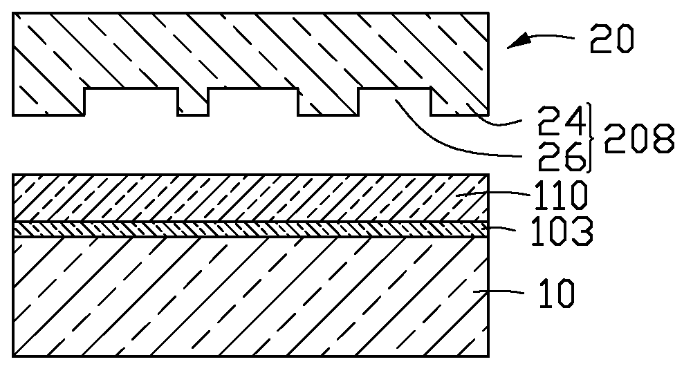
  • Nanoimprint resist, nanoimprint mold and nanoimprint lithography
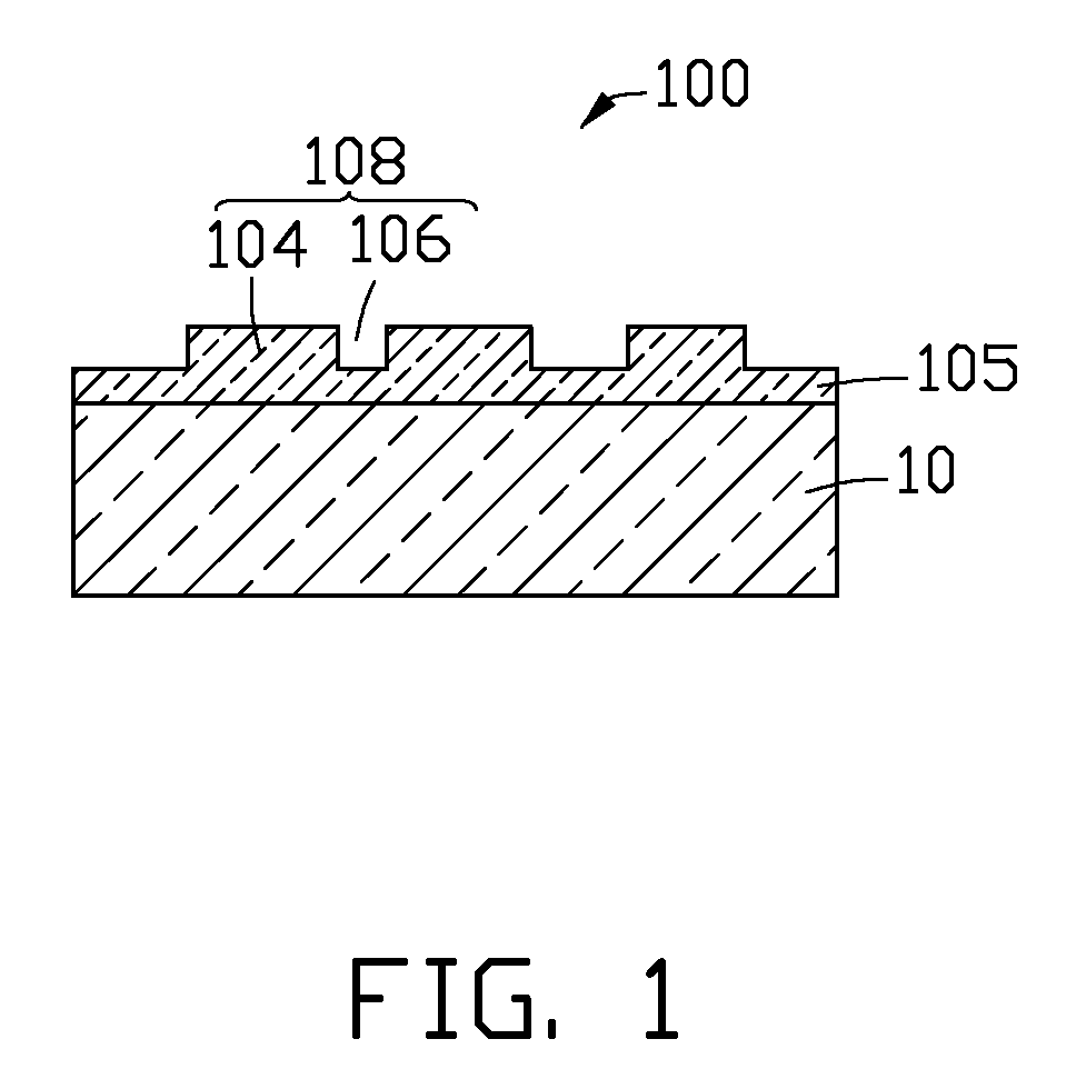
  • Nanoimprint resist, nanoimprint mold and nanoimprint lithography
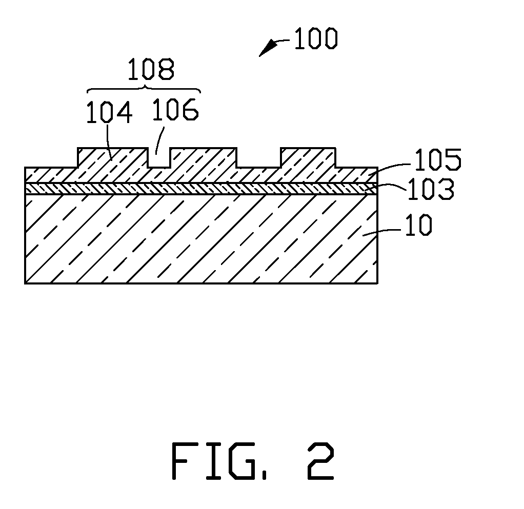
  • Nanoimprint resist, nanoimprint mold and nanoimprint lithography

Examples


Embodiment Construction

[0018]The disclosure is illustrated by way of example and not by way of limitation in the figures of the accompanying drawings in which like references indicate similar elements. It should be noted that references to “an” or “one” embodiment in this disclosure are not necessarily to the same embodiment, and such references mean at least one.

Nanoimprint Resist

[0019]A nanoimprint resist of one embodiment of includes a hyperbranched polyurethane oligomer (HP), a perfluoropolyether (PFPE), a methylmethacrylate (MMA), and a diluent solvent. In the nanoimprint resist, the weight percent (wt %) of the HP is in a range from about 50 wt % to about 60 wt %. The wt % of the PFPE is in a range from about 3 wt % to about 5 wt %. The wt % of the MMA is in a range from about 5 wt % to about 10 wt %. The wt % of the diluents solvent is in a range from about 25 wt % to about 35 wt %.

[0020]The chemical structure of the PFPE is

wherein m:n is in a range from about 0.6 to about 1.

[0021]If the nanoimprin...


PUM

PropertyMeasurementUnit
Fractionaaaaaaaaaa
Fractionaaaaaaaaaa
Fractionaaaaaaaaaa

Abstract

A nanoimprint resist includes a hyperbranched polyurethane oligomer (HP), a perfluoropolyether (PFPE), a methylmethacrylate (MMA), and a diluent solvent. A method of a nanoimprint lithography is also provided.

Description

RELATED APPLICATIONS[0001]This application is a continuation application of U.S. patent application Ser. No. 12 / 712,178, filed Feb. 24, 2010 entitled “NANOIMPRINT RESIST, NANOIMPRINT MOLD AND NANOIMPRINT LITHOGRAPHY” the disclosure of which is incorporated by reference.BACKGROUND[0002]1. Technical Field[0003]This disclosure relates to nanoimprint resisit, nanoimprint mold and nanoimprint lithography.[0004]2. Description of Related Art[0005]In fabrication of semiconductor integrated electrical circuits, integrated optical, magnetic, mechanical circuits and micro devices, and the like, are some of the key processing methods is the lithography. Lithography creates a pattern in a thin film located on a substrate, so that, in subsequent process steps, the pattern will be replicated in the substrate or in another material located on the substrate. Since the role of the thin film is to protect a part of the substrate in the subsequent replication steps, the thin film is called resist.[0006...

Claims


Application Information

Patent Timeline
IPC IPC(8): C23F1/00B29C59/00C08L63/00C08L75/04
CPCB82Y10/00B82Y40/00B29C59/026C08L63/00G03F7/0002C08G59/245Y10T428/31544Y10T428/31855
Inventor ZHU, ZHEN-DONGLI, QUN-QINGZHANG, LI-HUICHEN, MO
Owner TSINGHUA UNIV
Learn More