

Capacitive sensing assembly of touch panel
- Summary
- Abstract
- Description
- Claims
- Application Information
AI Technical Summary
Benefits of technology
Problems solved by technology
Method used
Image

Examples
Embodiment Construction
[0013]In order that those skilled in the art can further understand the present invention, a description will be provided in the following in details. However, these descriptions and the appended drawings are only used to cause those skilled in the art to understand the objects, features, and characteristics of the present invention, but not to be used to confine the scope and spirit of the present invention defined in the appended claims.
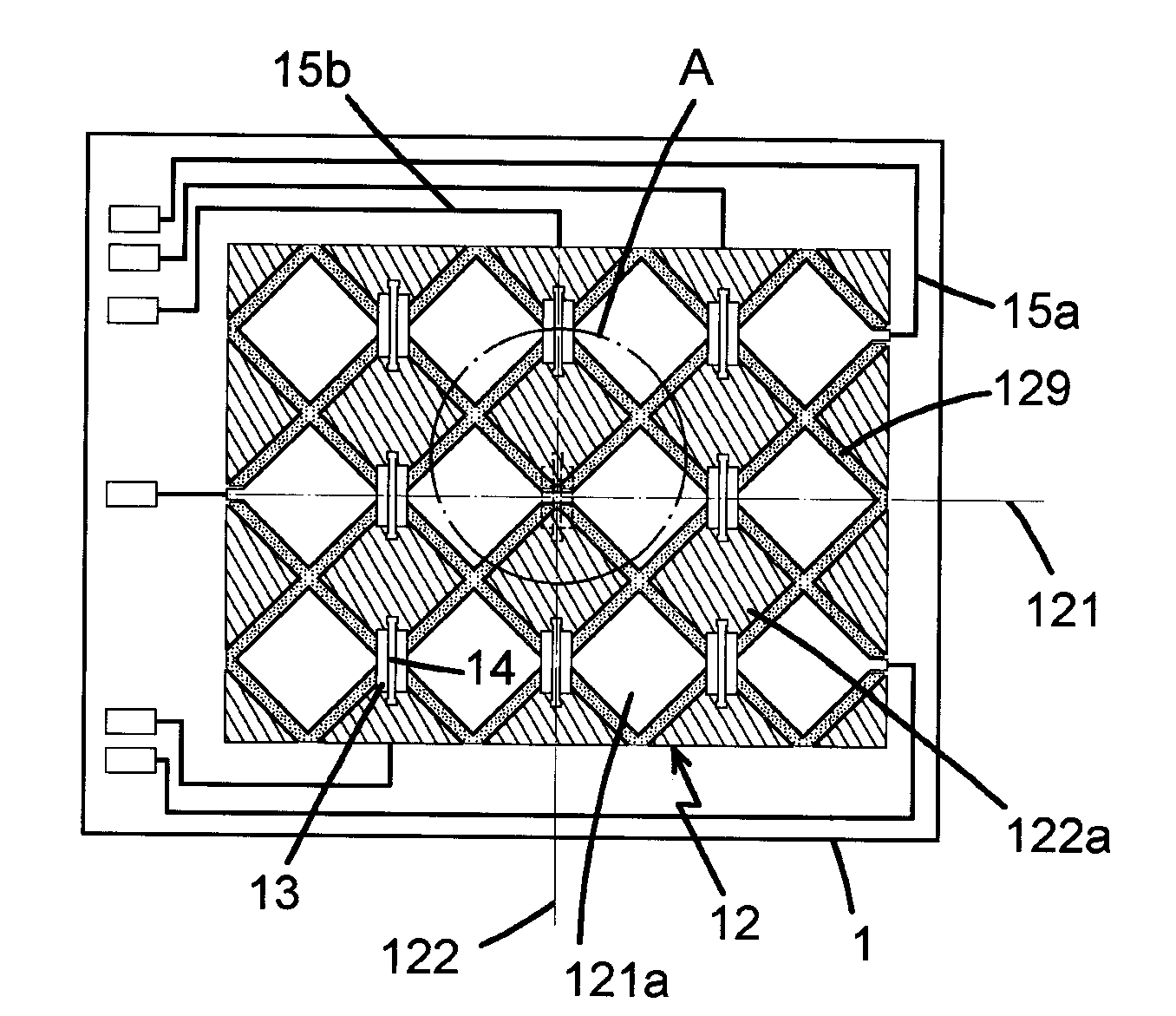
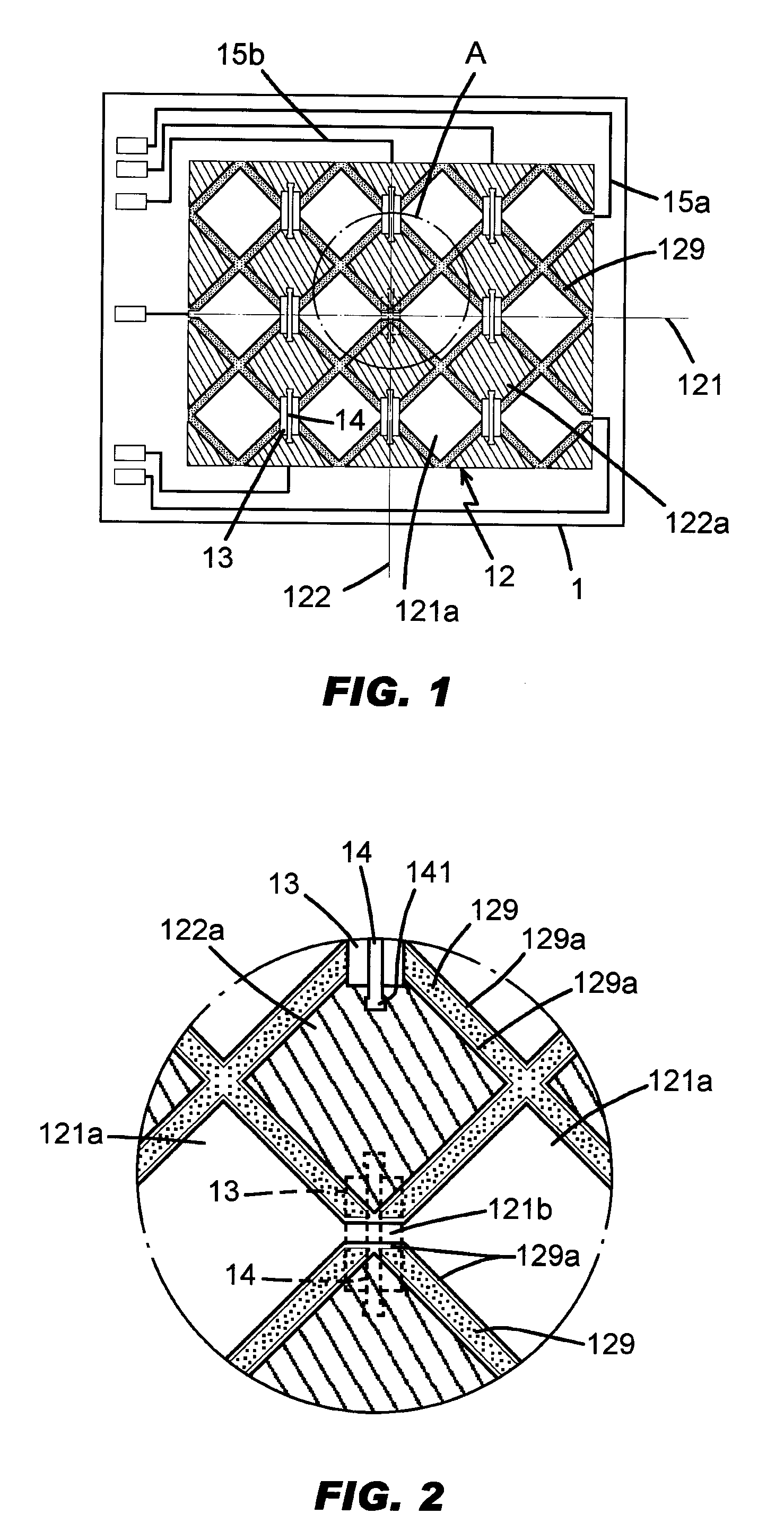
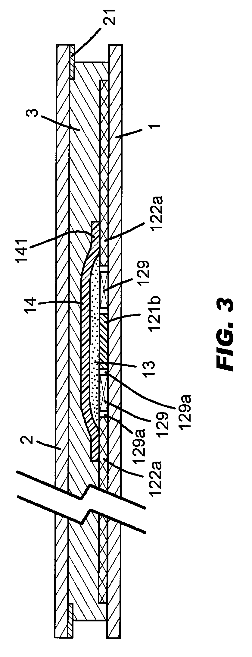
[0014]Referring to FIGS. 1 to 3, the preferred embodiment of the present invention is illustrated. The touch panel capacitive sensing assembly of the present invention includes a lower substrate 1 and an upper panel 2 which are combined by an adhering layer 3. A capacitive sensing layer 12 is adhered to the lower substrate 1 or the upper panel 2. The lower substrate 1 and upper panel 2 are made of high light transmission insulating thin glass plate. The adhering layer 3 is transparent UV glue. A periphery of the upper panel 2 is installed with colo...
PUM
 Abstract
Description
Claims
Application Information