Substrate for flip chip bonding and method of fabricating the same

a technology of substrate and flip chip, applied in the direction of resistive material coating, final product manufacturing, metallic pattern materials, etc., can solve the problems of difficult to relieve stress applied to metal posts, metal posts , limit the effect of realizing a circuit pattern having a fine pitch

Inactive Publication Date: 2010-12-16
SAMSUNG ELECTRO MECHANICS CO LTD
View PDF4 Cites 16 Cited by
  • Summary
  • Abstract
  • Description
  • Claims
  • Application Information

AI Technical Summary

Benefits of technology

[0013]Accordingly, the present invention has been made keeping in mind the problems encountered in the related art and the present invention intends to provide a substrate for flip chip bonding, which has improved impact resistance and mounting reliability, and a method of fabricating the same.

Problems solved by technology

As well, limitations are imposed on realizing a circuit pattern having a fine pitch.
Although the semiconductor substrate 10 for flip chip bonding according to the conventional technique is evaluated to be superior in terms of height uniformity and mounting reliability, it is not easy to relieve stress applied to the metal posts 18, and thus the metal posts 18 suffer from necking defects and mounting reliability is reduced.
As well, the above metal post structure employed in the conventional semiconductor substrate has a limitation in applying it to a package substrate on which the semiconductor substrate 10 is mounted.
This is because the formation of the metal posts having the same height is difficult when the metal posts are plated on the package substrate which warps in the manufacturing process unlike the silicon wafer 12.

Method used


Image

  • Substrate for flip chip bonding and method of fabricating the same
  • Substrate for flip chip bonding and method of fabricating the same
  • Substrate for flip chip bonding and method of fabricating the same

Examples


1st embodiment

1st Embodiment

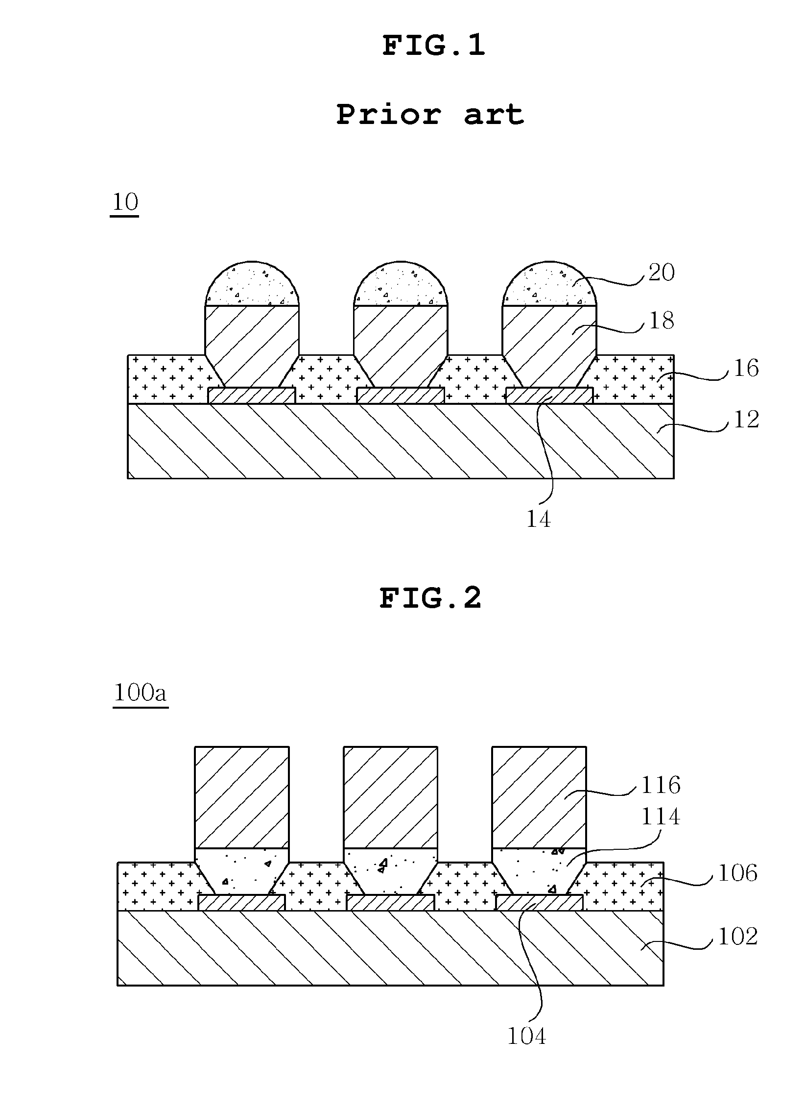
[0039]FIG. 2 is a cross-sectional view showing the substrate having metal posts according to a first embodiment of the present invention. Below, the substrate 100a having the metal posts according to the present embodiment is described with reference to the above drawing.

[0040]As seen in FIG. 2, the substrate 100a for flip chip bonding according to the present embodiment includes a base substrate 102, a solder resist layer 106, a base solder layer 114, and metal posts 116.

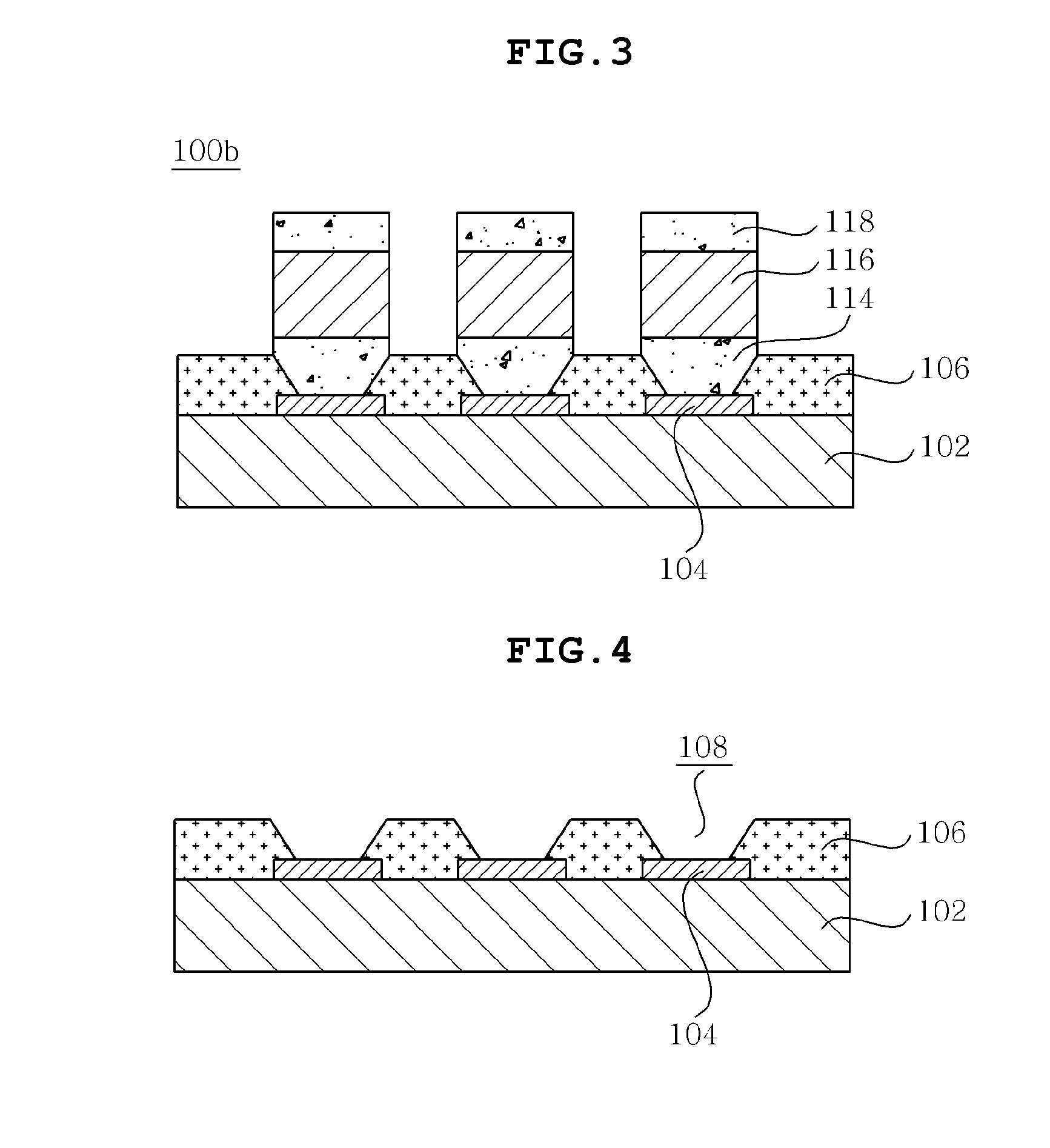
[0041]The base substrate 102 has pads 104 formed thereon, and the solder resist layer 106 having open portions 108 for exposing the pads 104 is formed on the base substrate 102. Examples of the base substrate 102 may include a semiconductor substrate and a package substrate.

[0042]The base solder layer 114 functions to relieve impact applied to the metal posts 116 and improve height uniformity and mounting reliability, and is formed on the pads 104.

[0043]The metal posts 116 enable the fine pitching of ...

2nd embodiment

2nd Embodiment

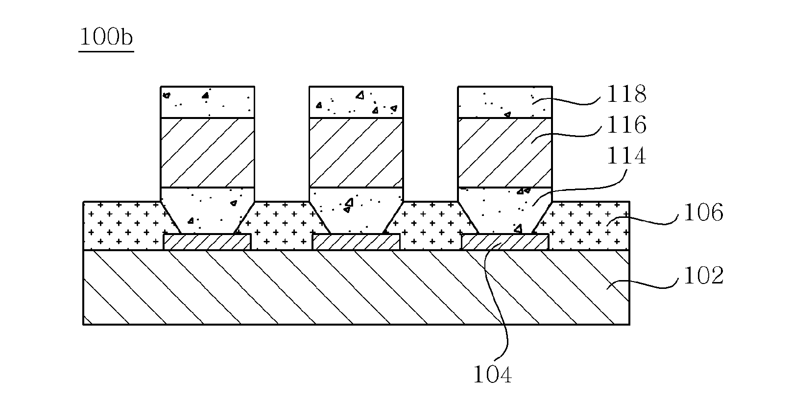
[0047]FIG. 3 is a cross-sectional view showing a substrate for flip chip bonding according to a second embodiment of the present invention. In the description of the second embodiment, elements which are the same as or similar to those of the first embodiment are designated by the same reference numerals, and redundant descriptions are omitted.

[0048]As shown in FIG. 3, the substrate 100b for flip chip bonding according to the second embodiment is configured such that solder caps 118 are formed on the metal posts 116 of the substrate 100a of FIG. 2.

[0049]The solder caps 118 produce a buffering effect upon packaging of the substrate for flip chip bonding and also assure height uniformity.

[0050]Also, in order to enhance the force of adhesion between the metal posts 116 and the solder caps 118, a second surface treatment layer (not shown) is thinly formed therebetween, which is composed of a Ni plating layer or a Ni alloy plating layer with or without thereon any one selec...


PUM

PropertyMeasurementUnit
thicknessaaaaaaaaaa
temperatureaaaaaaaaaa
photosensitiveaaaaaaaaaa

Abstract

Disclosed is a substrate for flip chip bonding, in which a base solder layer is formed between a pad and a metal post, thereby increasing impact resistance and mounting reliability. A method of fabricating the substrate for flip chip bonding is also provided.

Description

CROSS REFERENCE TO RELATED APPLICATION[0001]This application claims the benefit of Korean Patent Application No. 10-2009-0051605, filed Jun. 10, 2009, entitled “Substrate of flip chip and fabricating method of the same”, which is hereby incorporated by reference in its entirety into this application.BACKGROUND OF THE INVENTION[0002]1. Technical Field[0003]The present invention relates to a substrate for flip chip bonding and a method of fabricating the same.[0004]2. Description of the Related Art[0005]With the recent advancement of the electronics industry, there is a demand for increasing performance and functionality of electronic components and reducing the size thereof. Accordingly, high integration, slimness and fine circuit patterning are also required on a substrate for surface mounting components, such as SIP (System in Package), 3D package, etc.[0006]In particular, in techniques for mounting electronic components on the surface of a substrate, a wire bonding process or a fl...

Claims


Application Information

Patent Timeline
Patent Type & Authority Applications(United States)
IPC IPC(8): H05K1/09B05D5/12
CPCH01L24/11H01L24/13H01L2224/1146H01L2224/1147H01L2224/11901H01L2224/13022H01L2224/1308H01L2224/13083H01L2224/13084H01L2224/131H01L2224/13111H01L2224/13144H01L2224/13147H01L2224/13155H01L2224/13164H01L2224/16H01L2924/01029H01L2924/01046H01L2924/01078H01L2924/01079H01L2924/01327H05K3/243H05K3/3436H05K3/3484H05K2201/1025H01L2924/00014H01L2924/014H01L2924/00013H01L2924/01005H01L2924/01006H01L2924/01019H01L2924/01033H01L2924/01047H01L2224/13099H01L23/49811Y02P70/613H01L2224/05022H01L2224/05026H01L2224/05568H01L2224/05001H01L2224/05144H01L2224/05155H01L2224/05164H01L2224/05611H01L2224/05644H01L2224/05647H01L2224/05655Y10T29/49147Y10T29/49165H01L2924/12042H01L2924/00H01L24/05H01L24/03H01L2224/023H05K3/3485Y02P70/50H01L2924/0001
Inventor OH, HUENG JAECHUNG, TAE JOONLEE, DONG GYUMUN, SEON JAECHOI, JIN WON
Owner SAMSUNG ELECTRO MECHANICS CO LTD
Why Eureka
Try Eureka