Semiconductor device

a technology of semiconductors and devices, applied in the direction of semiconductor devices, basic electric elements, electrical equipment, etc., can solve the problems of difficult ionization, adversely affecting transistor characteristics, and affecting the efficiency of transistors, and achieves high precision, high reliability, and efficient ionization.

Inactive Publication Date: 2010-12-16
SHARP KK
View PDF1 Cites 45 Cited by
  • Summary
  • Abstract
  • Description
  • Claims
  • Application Information

AI Technical Summary

Benefits of technology

[0010]The present invention has been achieved in view of the above conventional problems, and an object thereof is to provide a semiconductor device that is capable of controlling the location of impact ionization with ease and high precision and efficiently absorbing generated electrons and holes, thereby achie

Problems solved by technology

If an electrode having Schottky characteristics is directly joined to a nitride semiconductor, a Schottky leakage current may be generated and may adversely affect the transistor characteristics.
However, in some cases, conventional MISFETs may induce impact ionization (a phenomenon in which electrons accelerated by an electric field collide with the crystal lattice, thereby producing electrons and holes) in a channel that corresponds to the gate electrode.
The holes caused by such impact ioni

Method used


Image

  • Semiconductor device
  • Semiconductor device
  • Semiconductor device

Examples


first embodiment

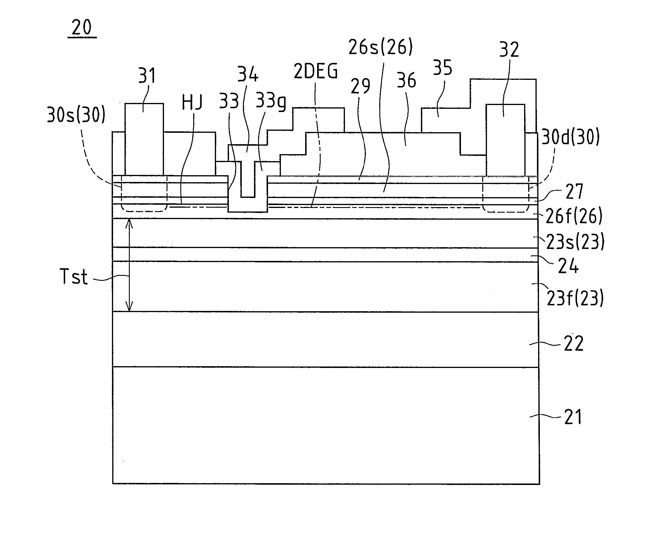
[0057]A semiconductor device and a manufacturing method therefor according to the present embodiment will be described with reference to FIGS. 1 to 10.

[0058]FIG. 1 is a diagrammatic cross-sectional view diagrammatically illustrating the general configuration of a semiconductor device according to a first embodiment of the present invention. Note that any hatching indicating the cross-sectional plane is omitted for the visibility of the drawing (the same applies to the following drawings).

[0059]One example of a semiconductor device 20 according to the present embodiment is a field-effect transistor (MOSFET) having a compound semiconductor MOS structure.

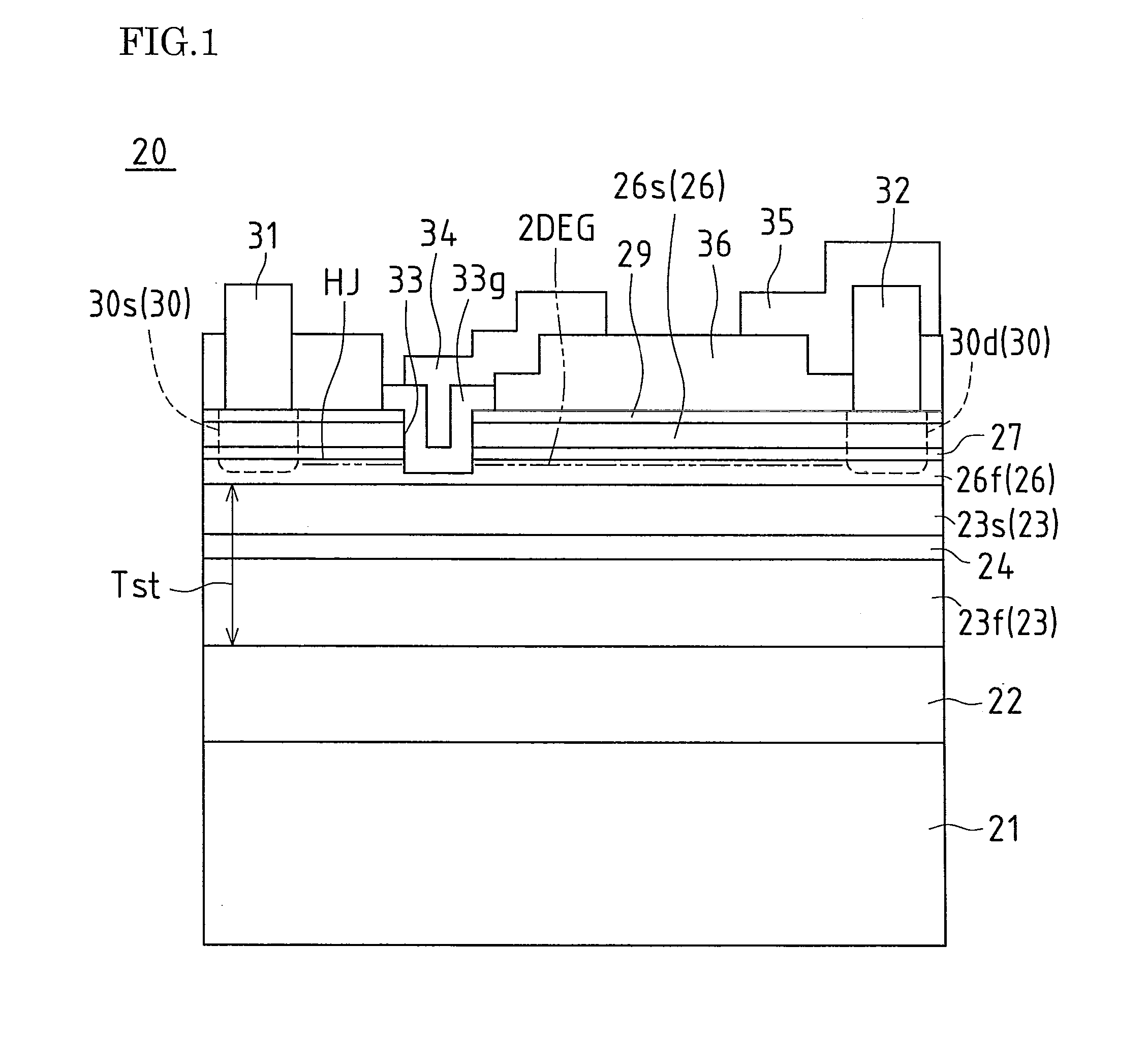
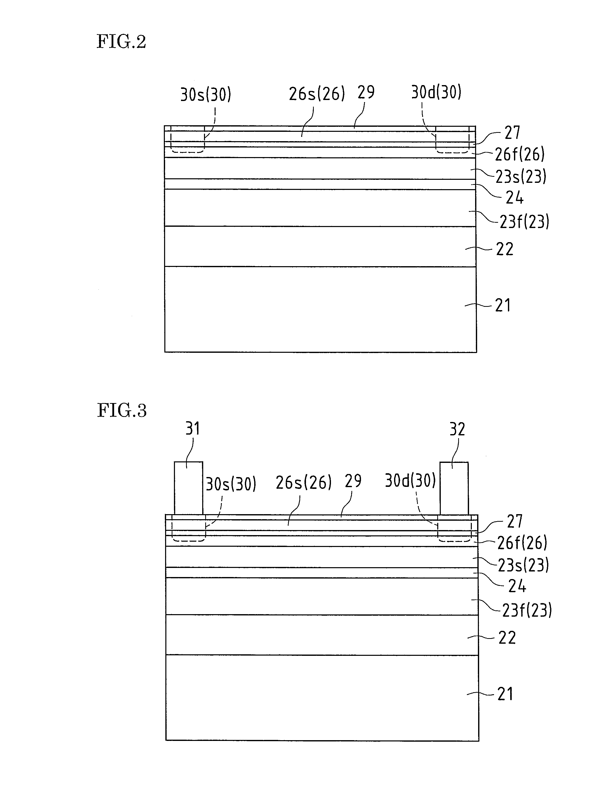
[0060]The semiconductor device 20 includes multiple layers layered in sequence on a substrate 21, namely a buffer layer 22, a base compound semiconductor layer 23f (base compound semiconductor layer 23), an impact ionization control layer 24, a base compound semiconductor layer 23s (base compound semiconductor layer 23), a channel defi...

second embodiment

[0129]A semiconductor device according to the present embodiment will be described with reference to FIG. 11. Note that, since the occurrence and effect of impact ionization are as described in the first embodiment and the basic configuration is similar to that of the semiconductor device 20, different points are mainly described herein.

[0130]FIG. 11 is a diagrammatic cross-sectional view diagrammatically illustrating a general configuration of a semiconductor device according to a second embodiment of the present invention.

[0131]One example of a semiconductor device 40 according to the present embodiment is a field-effect transistor having a compound semiconductor MOS structure.

[0132]The semiconductor device 40 includes multiple layers layered in sequence on a substrate 41, namely a buffer layer 42, a base compound semiconductor layer 43f (base compound semiconductor layer 43), an impact ionization control layer 44, a base compound semiconductor layer 43s (base compound semiconduct...

third embodiment

[0162]A semiconductor device according to the present embodiment will be described with reference to FIG. 12. Note that, since the occurrence and effect of impact ionization are as described in the first and second embodiments and the basic configuration is similar to those of the semiconductor devices 20 and 40, different points are mainly described herein.

[0163]FIG. 12 is a diagrammatic cross-sectional view diagrammatically illustrating a general configuration of a semiconductor device according to a third embodiment of the present invention.

[0164]One example of a semiconductor device 60 according to the present embodiment is a field-effect transistor having a compound semiconductor MOS structure.

[0165]The semiconductor device 60 according to the present embodiment includes multiple layers layered in sequence on a substrate 61, namely a buffer layer 62, a base compound semiconductor layer 63f (base compound semiconductor layer 63), an impact ionization control layer 64, a base com...


PUM


Abstract

One embodiment of a semiconductor device according to the present invention includes a substrate, a base compound semiconductor layer layered on the substrate to form a base, a channel defining compound semiconductor layer layered on the base compound semiconductor layer to define a channel, and an impact ionization control layer that is layered within a layering range of the base compound semiconductor layer and controls the location of impact ionization, wherein the base compound semiconductor layer is formed of a first compound semiconductor, the channel defining compound semiconductor layer is formed of a second compound semiconductor, and the impact ionization control layer is formed of a third compound semiconductor that has a smaller band gap than the first compound semiconductor.

Description

CROSS-REFERENCE TO RELATED APPLICATIONS[0001]This application claims priority under 35 U.S.C. §119(a) on Patent Application No. 2009-140271 filed in Japan on Jun. 11, 2009, the entire contents of which are herein incorporated by reference.BACKGROUND OF THE INVENTION[0002]1. Field of the Invention[0003]The present invention relates to a semiconductor device that includes an impact ionization control layer that controls the location of impact ionization.[0004]2. Related Art[0005]Semiconductor devices (nitride semiconductor devices) using nitride semiconductors have large dielectric breakdown electric fields, excellent heat resistance, and high electron saturation drift velocity, so that they can provide electronic devices that are excellent in terms of high-temperature or high-power operation, for example, as compared to Si- or GaAs-based devices. For this reason, the development of semiconductor devices using nitride semiconductors is being pursued.[0006]For example, for the manufact...

Claims


Application Information

Patent Timeline
IPC IPC(8): H01L29/778
CPCH01L29/1083H01L29/2003H01L29/402H01L29/4236H01L29/66462H01L29/7783H01L29/7787
Inventor ITO, NOBUYUKITWYNAM, JOHN KEVIN
Owner SHARP KK
Why Eureka
Try Eureka