
Semiconductor device

Inactive Publication Date: 2010-12-16
RENESAS ELECTRONICS CORP
View PDF1 Cites 39 Cited by
  • Summary
  • Abstract
  • Description
  • Claims
  • Application Information

AI Technical Summary

Benefits of technology

[0010]In light of the above-mentioned problems, the present invention has been made, and an object thereof is to provide a semiconductor device which scarcely malfunctions even when the device is used as a high-side element, and can keep a high breakdown voltage.
[0012]According to the aspect of the invention, the first conductive type first region and second region are isolated electrically from each other by the second conductive type fifth region. Therefore, even when the semiconductor device is used as a high-side element, malfunctions thereof can be reduced.
[0014]Further, the sixth region, which has a higher impurity concentration than that of the second region, is formed between the fifth region and the second region. The sixth region restrains the depletion layer, which is spread from the pn junction between the third and second regions toward the second region by the reverse bias, from linking with a depletion layer generated in the pn junction between the fifth and sixth regions. In this way, the generation of punchthrough is restrained so that the semiconductor device can keep a high breakdown voltage.

Problems solved by technology

However, the first structure is not any RESURF structure; thus, when a reverse bias is applied thereto, an electric field concentrates into the vicinity of a junction between the p-type body region and the n-type drift region, thereby resulting in a problem that the structure has a lower breakdown voltage than the above-mentioned RESURF structure having no n-type isolation region.
However, the decrease results in a rise in the on-resistance of the transistor.
As a result, there is caused a problem that the element size should be made large.
As a result thereof, electric-field-concentration is caused in the vicinity of the junction between the p-type body region and the n-type drift region, thereby causing a problem that the structure has a lower breakdown voltage than the above-mentioned RESURF structure having no n-type isolation region.

Method used


Image

  • Semiconductor device
  • Semiconductor device
  • Semiconductor device

Examples


embodiment 1

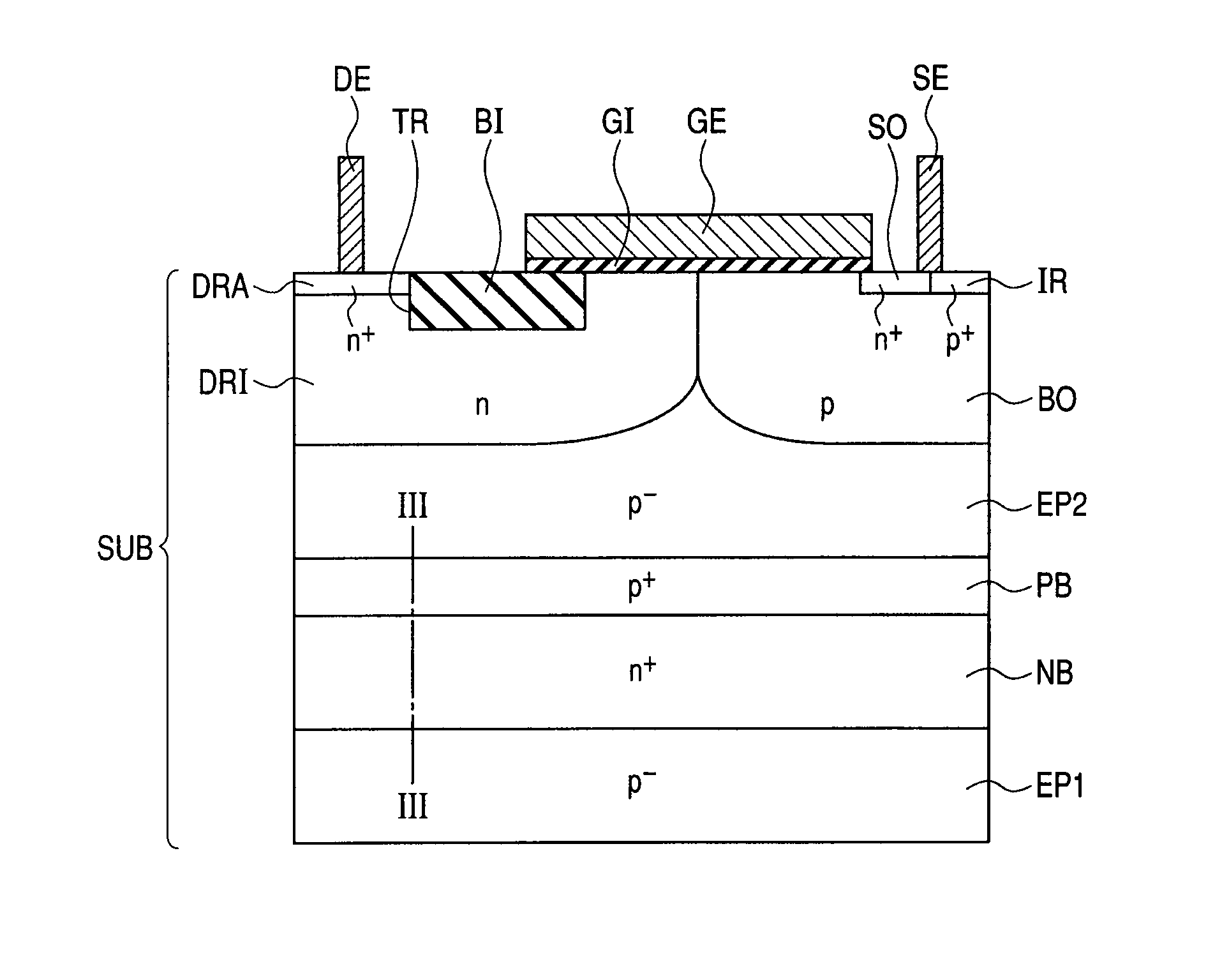
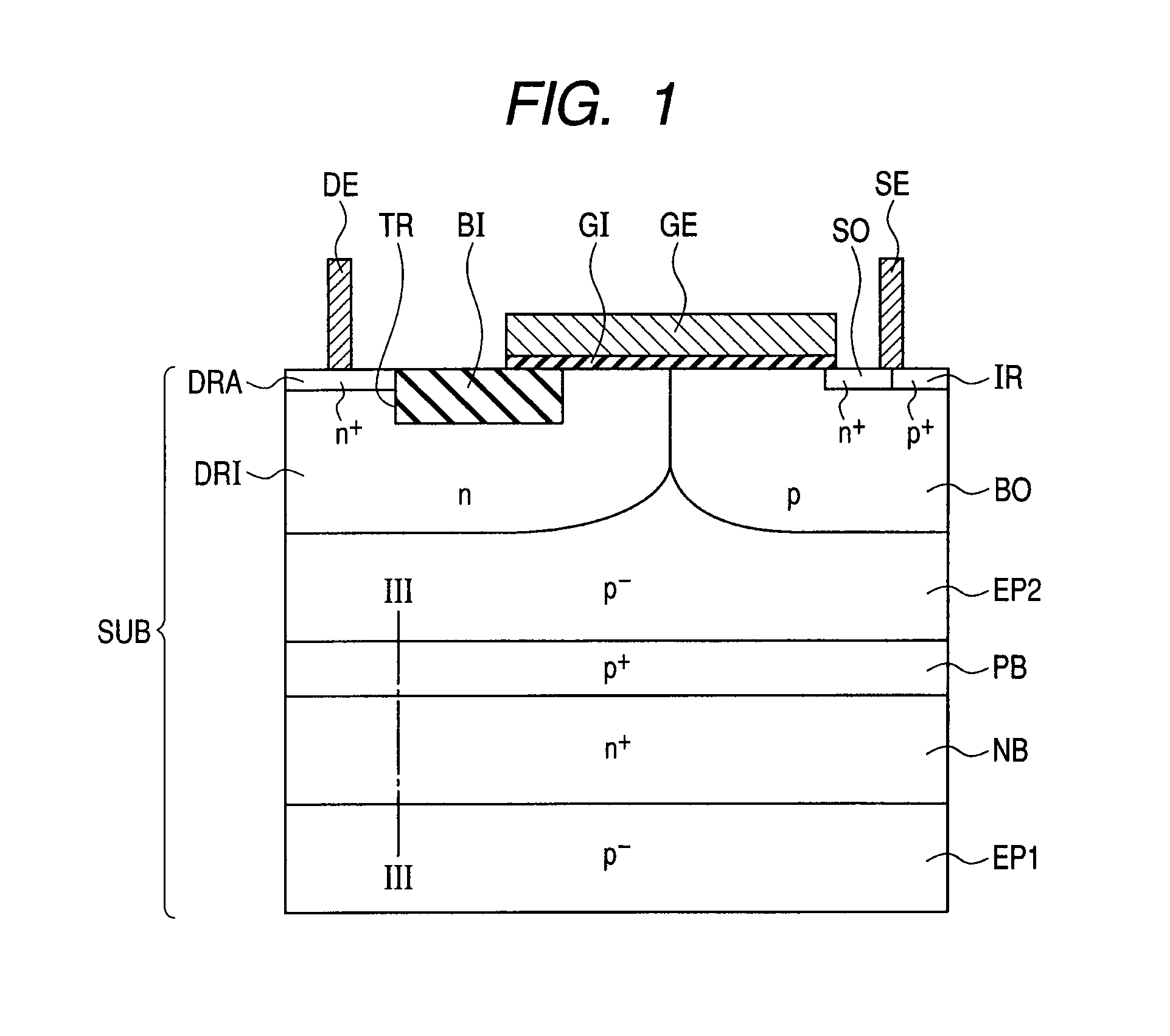
[0046]First, the structure of a semiconductor device of the present embodiment will be described with reference to FIG. 1.

[0047]As illustrated in FIG. 1, the semiconductor device of the embodiment has, for example, an LDMOS transistor. This semiconductor device mainly has a semiconductor substrate SUB, a p− epitaxial region (first region) EP1, an n+ buried region (fifth region) NB, a p+ buried region (sixth region) PB, a p− epitaxial region (second region) EP2, an n-type drift region (third region) DRI, a p-type body region (fourth region) BO, an n+ drain region DRA, an n+ source region, a gate electrode layer GE, and an STI structure TR and BI.

[0048]The semiconductor substrate SUB includes, for example, silicon. The semiconductor substrate SUB has a main surface (the upper surface of the substrate in FIG. 1). Inside the semiconductor substrate SUB, the p− epitaxial region EP1 is formed.

[0049]The p− epitaxial region EP2 is formed inside the semiconductor substrate SUB and at the mai...

embodiment 2

[0085]In an analog / digital consolidated technique, an LDMOS transistor as in Embodiment 1 may be formed together with a complementary MOS (CMOS), a bipolar transistor, a diode, a memory element and others on a single chip through the same process. When the transistor or transistors of Embodiment 1 are laid out on such a chip, it is necessary to isolate the transistor(s) electrically from the other elements. In the present embodiment, a structure for the electrical isolation will be described with reference to FIGS. 19 and 20.

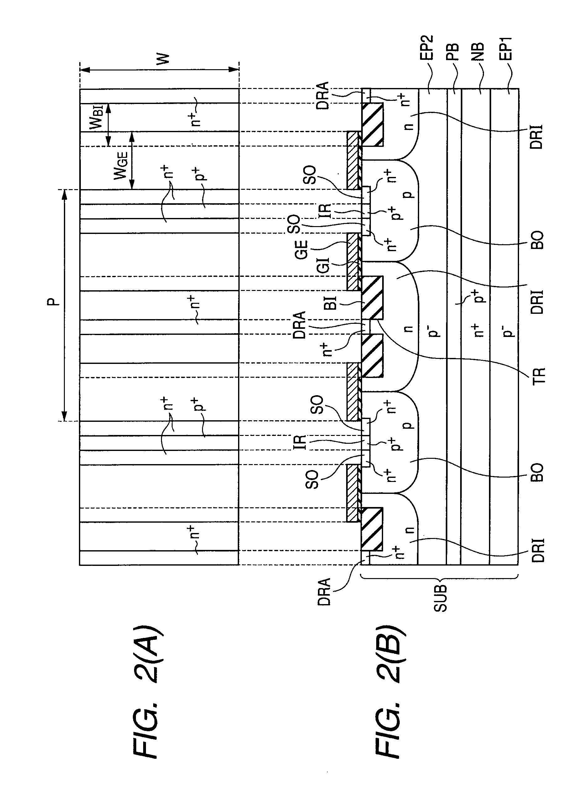
[0086]As illustrated in FIGS. 19 and 20, in the embodiment, an n-type isolation region (impurity region for isolation) SR is formed so as to surround the circumference of an area ARA when the structure of the embodiment is viewed from the above, the area ARA being an area where an array of LDMOS transistors as illustrated in FIGS. 2(A) and 2(B) is arranged. The n-type isolation region SR is formed in a semiconductor substrate SUB to be combined with a p− epitaxi...

embodiment 3

[0090]As illustrated in FIG. 21 and FIG. 22, in the present embodiment, a trench isolation is formed for isolating an area ARA where an array of LDMOS transistors is arranged electrically from other elements. The trench isolation has an isolating trench TRS and a buried (or filled) insulating layer BIS.

[0091]The isolating trench TRS surrounds the circumference of the LDMOS-transistor-array-arranged area ARA when the structure of the embodiment is viewed from the above. The isolating trench TRS penetrates from the main surface of the present semiconductor substrate SUB through a p+ buried region PB to reach an n+ buried region NB.

[0092]It is preferred that the isolating trench TRS penetrates through the n+ buried region NB also to reach a p− epitaxial region EP1. The penetration of the isolating trench TRS through the n+ buried region NB, as described herein, makes it possible to make the n+ buried region NB so as to have a floating potential.

[0093]The buried insulating layer BIS is ...


PUM


Abstract

Provided is a semiconductor device which scarcely malfunctions even when the device is used as a high-side element, and can keep a high breakdown voltage. In a semiconductor substrate having a main surface, a first p− epitaxial region is formed. At the main surface side of the first p− epitaxial region, a second p− epitaxial region is formed. At the main surface side of the second p− epitaxial region, an n-type drift region and a p-type body region are formed. Between the first and second p− epitaxial regions, an n+ buried region having a floating potential is formed to isolate these regions electrically from each other. Between n+ buried region and the second p− epitaxial region, a p+ buried region is formed which has a higher p-type impurity concentration than the second p− epitaxial region.

Description

CROSS-REFERENCE TO RELATED APPLICATIONS[0001]The disclosure of Japanese Patent Application No. 2009-143591 filed on Jun. 16, 2009 including the specification, drawings and abstract is incorporated herein by reference in its entirety.BACKGROUND OF THE INVENTION[0002]The present invention relates to a semiconductor device, in particular, a semiconductor device having a lateral element.[0003]A general structure of a high-breakdown-voltage laterally diffused metal oxide semiconductor (MOS) transistor (LDMOS transistor) is the structure of a reduced surface field (RESURF) MOS transistor (see FIG. 1 in Non-patent document 1 (see below)). In the case of optimizing, in this structure, the profile of the concentration of impurities in its n-type drift region, a depletion layer spreads also in a junction between the n-type drift region and a p− epitaxial region underneath the region when a reverse vias is applied to the structure. As a result, the structure can have a high breakdown voltage.[...

Claims


Application Information

Patent Timeline
IPC IPC(8): H01L29/78
CPCH01L27/0635H01L27/0922H01L29/0653H01L29/0692H01L29/0834H01L29/0847H01L29/861H01L29/1083H01L29/1087H01L29/6609H01L29/66659H01L29/7393H01L29/7835H01L29/10
Inventor YANAGI, SHINICHIRO
Owner RENESAS ELECTRONICS CORP
Learn More