Memory architecture with a current controller and reduced power requirements

a memory architecture and controller technology, applied in the direction of information storage, static storage, digital storage, etc., can solve the problems of increasing design cycle time and manufacturing costs, reducing read time and power requirements, and previously used 3t or more recent 1t architectures are not functionally capable, so as to reduce power consumption, reduce read time and power requirements, and reduce power consumption

Active Publication Date: 2010-12-16
LYNCH JOHN K
View PDF14 Cites 12 Cited by
  • Summary
  • Abstract
  • Description
  • Claims
  • Application Information

AI Technical Summary

Benefits of technology

[0034]Cancelling the uncertain effect of hold node transistor threshold voltage by using a differential pair construct enables smaller intervals between voltages on the storage mechanism or greater signal drift before requiring a refresh. For writing, using smaller voltage intervals allows smaller amplitude voltage transitions on the write bit line, reducing power consumption. Greater allowable signal drift makes the time between refreshes for each bit cell longer, reducing power consumption.
[0035]Isolating the storage mechanism from the read bit line eliminates the need for storage mechanism restore and provides the advantage of a nondestructive read. In this way both the read time and power requirements are reduced.
[0036]Eliminating large standard logic voltage transitions on the read bit line by using an amplifying structure that senses the voltage change on the read bit line and transforms the voltage change to a binary value on a wire that is distinct from the read bit line and decoupled from the capacitance associated with the read bit line reduces power requirements.
[0037]Providing a mechanism to indicate the appropriate stop time and modifications to the structure to allow the current in the bit cell to stop at a point after the voltage change on the read bit line is deemed significant and before an inherent limit due to circuit topology is reached additionally reduces power requirements.
[0038]Using multiple reference signals to control the change on the read bit line by using a plurality of input reference levels facilitates a multi-bit cell.
[0039]Reading a value representing multiple bits from a storage mechanism reduces memory size requirements while reducing power requirements.

Problems solved by technology

Both of these architectures have several well-known limitations and inherent drawbacks.
These needs increase design cycle time and manufacturing costs.
Neither the previously used 3T nor the more recent 1T architectures are functionally capable of meeting this need.
This difference in voltage is small and read from a floating bit line thereby making it susceptible to noise.
The noise factor makes it impractical to represent multiple bits per storage mechanism.
While the three storage mechanisms allow multi-bit storage within a single cell, the power consumption of such a system is similar to the combined power consumption of three single bit cells.
U.S. Pat. No. 7,133,311 to Liu (incorporated herein by reference) discloses a method, based on a 1T architecture, of sensing three voltage levels representing 1.5 bits per storage mechanism however, it is limited to the noise sensitivity of the 1T architecture.
In fact, U.S. Pat. No. 7,133,311 teaches away from the notion of using four levels, concluding that such arrangement would not be feasible due to increased noise.

Method used


Image

  • Memory architecture with a current controller and reduced power requirements
  • Memory architecture with a current controller and reduced power requirements
  • Memory architecture with a current controller and reduced power requirements

Examples


Embodiment Construction

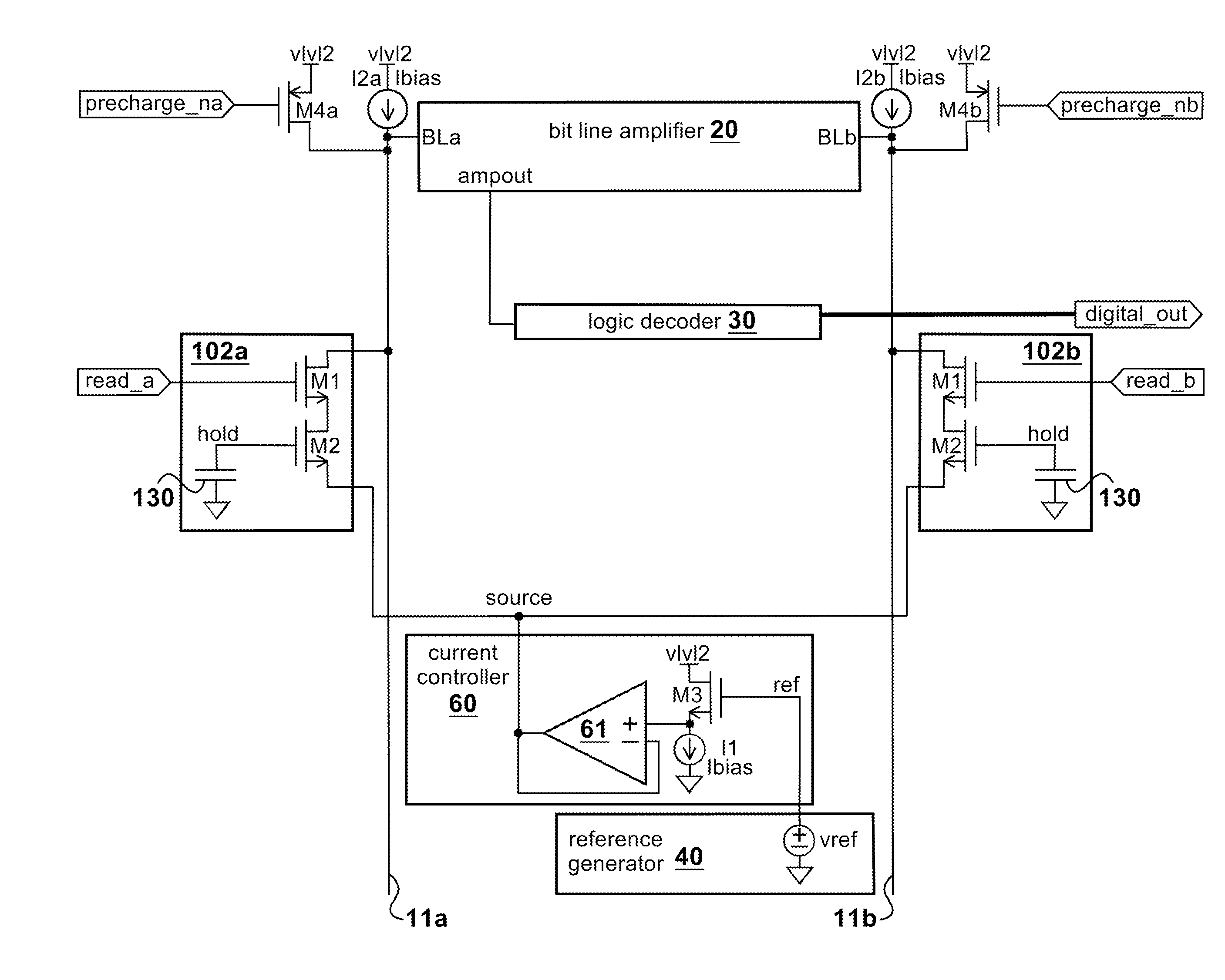
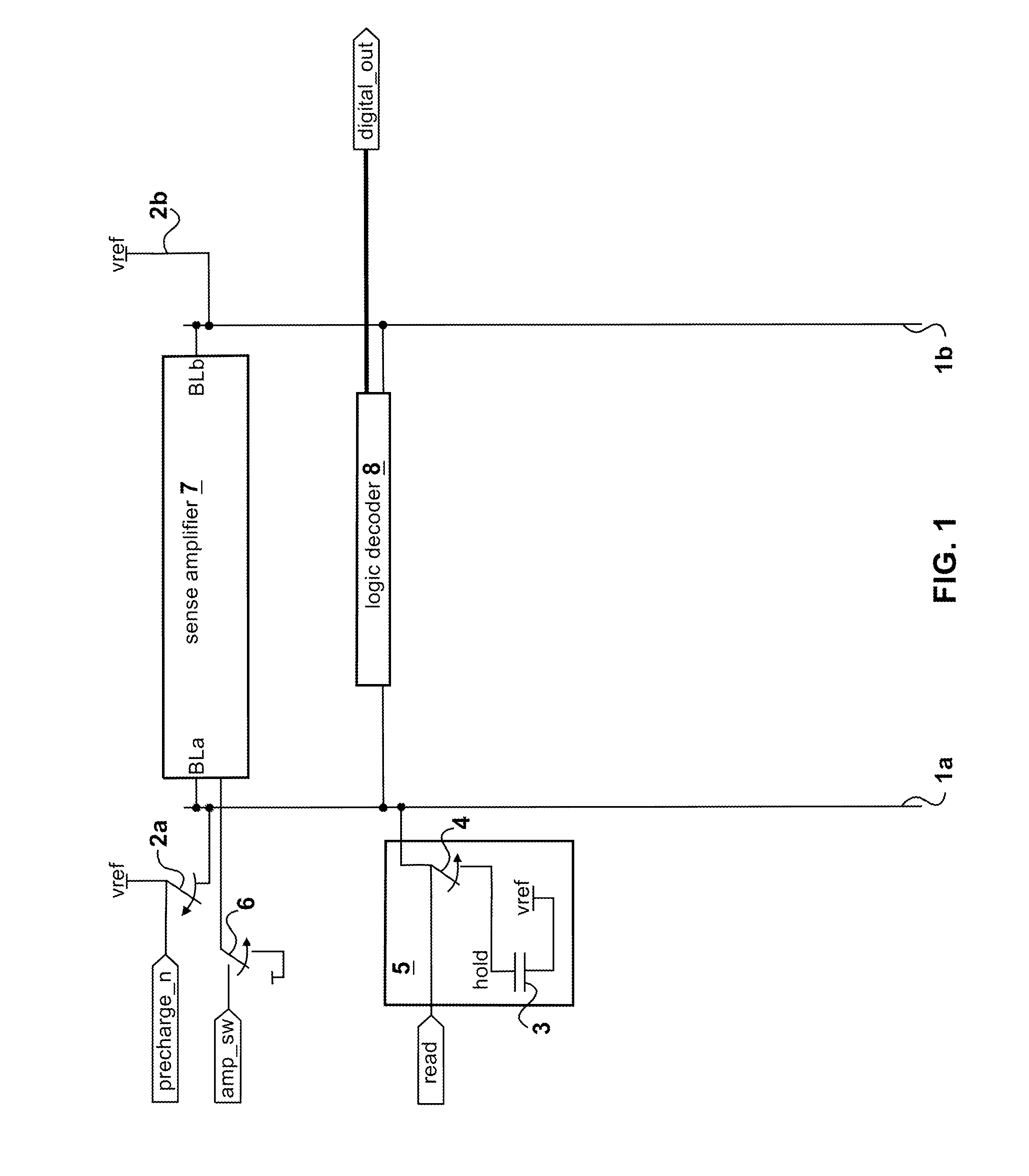
[0127]To better understand the inventive concept and its departure from the prior art, a brief review of the prior art will be instructive.

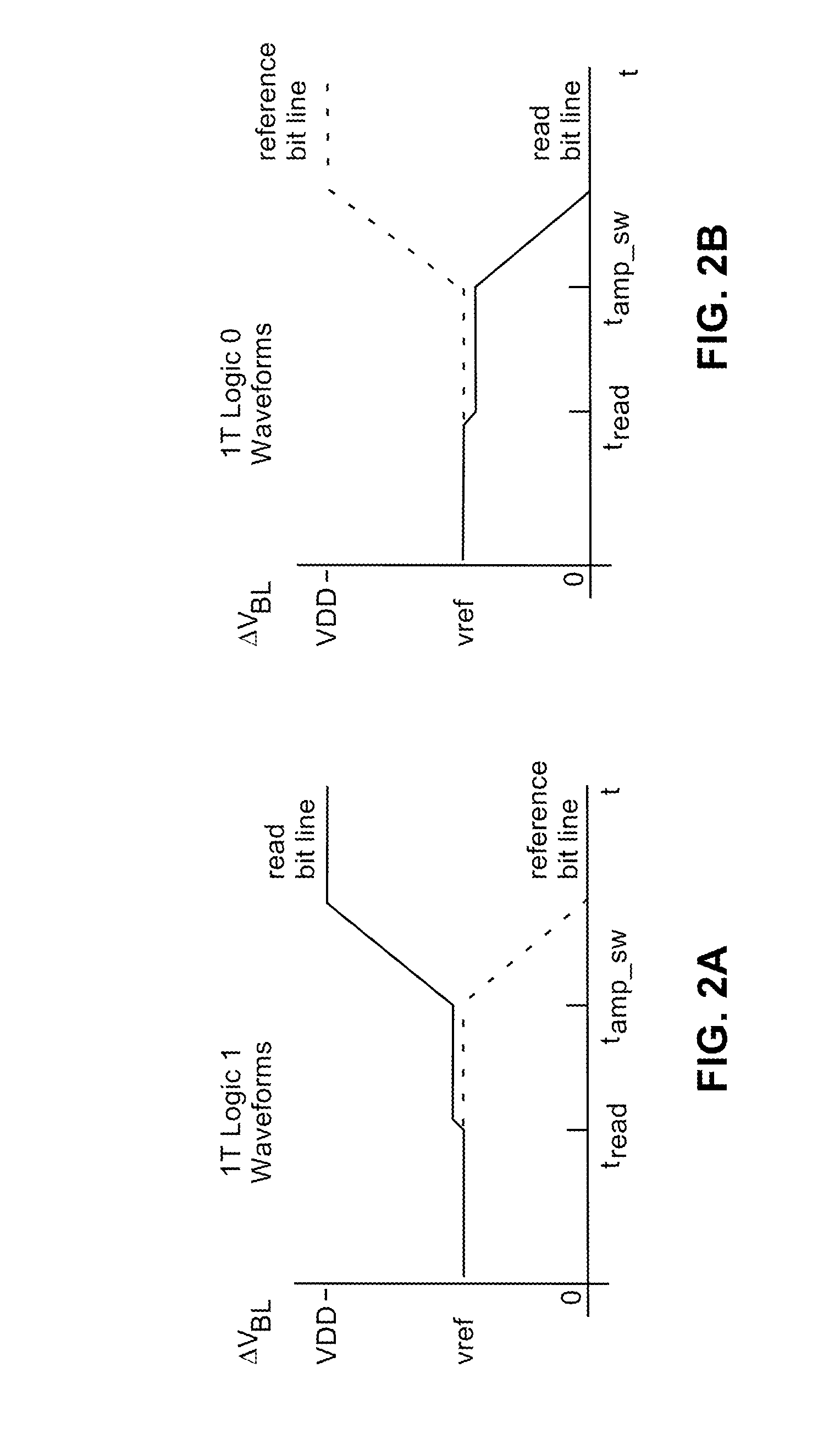
[0128]FIG. 1 shows a block diagram for a common 1T structure of prior art. The read process of the 1T consists of the following basic steps. In the initial condition, the closed precharge input switch 2a causes the read bit line 1a to hold to the voltage value vref. At the start of a read, the precharge input switch 2a opens causing the read bit line to float at vref. Next, the read input to bit cell 5 is asserted and the switch 4 in bit cell 5 closes. The charge on the storage capacitor 3 in bit cell 5 is shared with the charge on the read bit line and the voltage of the read bit line is defined as

ΔVBL=(vhold−vref)*(CS / (CS+CBL))  (Eq. 1)[0129]where ΔVBL=VBL−vref, VBL is the read bit line voltage referenced to ground, vref is a reference power supply input and vhold is the voltage on the hold node, CS is the value of the bit cell capacitor, CBL i...


PUM


Abstract

Disclosed is a memory architecture comprising at least one memory bit cell and at least one read bit line whose voltage is controlled and changed by a current from a current controller. Each memory bit cell has a storage mechanism, a controlled current source, and a read switch. The controlled current source in each memory bit cell is electrically connected to the read bit line through the read switch. The current from the current controller that controls and changes the read bit line voltage flows through the controlled current source in the memory bit cell. The value of this current is determined by a function of a difference between the voltage on the storage mechanism in the memory bit cell and a reference voltage from a reference voltage input to the current controller. In some versions an indicator is provided for indicating when to stop the current in the controlled current source that controls a voltage change on one of the read bit lines. The indicator has an on and an off condition and a switch is provided for stopping the current in the controlled current source when the indicator is activated in the on condition. The current in the controlled current source is stopped when the voltage change on the read bit line is greater than a predetermined threshold.

Description

PRIORITY AND RELATED APPLICATIONS[0001]This application claims the benefit of priority from provisional application U.S. Ser. No. 61 / 154,241 filed Feb. 20, 2009. This application is incorporated by reference herein in its entirety.BACKGROUND OF THE INVENTION[0002]1. Field of Invention[0003]This invention relates to the field of solid state devices for information storage and in particular for a method and structure to solve the problem of noise sensitivity and to reduce power consumption in reading the voltage stored on a bit cell in a random access memory.[0004]2. Background of the Related Art[0005]Dynamic random access memory, DRAM, is a type of random access memory that stores data in bit cells within an integrated circuit. A bit cell typically includes one capacitor as the storage mechanism. Broadly speaking the read process used in DRAM technology takes the analog voltage data stored in the bit cell, translates it into a standard digital logic voltage, makes this voltage availa...

Claims


Application Information

Patent Timeline
Patent Type & Authority Applications(United States)
IPC IPC(8): G11C11/24G11C5/14G11C7/10G11C7/06
CPCG11C11/404G11C11/405G11C11/4076G11C11/4091G11C11/4099G11C11/565G11C7/08G11C5/14G11C7/12G11C11/4074G11C11/4094
Inventor LYNCH, JOHN
Owner LYNCH JOHN K
Why Eureka
Try Eureka