Optical Interconnection Arrangement For High Speed, High Density Communication Systems

a communication system and high-speed technology, applied in the field of optical interconnection arrangement, can solve the problems of consuming a significant amount of power, interconnecting computer servers or network nodes that cannot keep up with the growth of computing power,

Active Publication Date: 2010-12-16
CISCO TECH INC
View PDF17 Cites 25 Cited by
  • Summary
  • Abstract
  • Description
  • Claims
  • Application Information

AI Technical Summary

Benefits of technology

[0008]The needs remaining in the prior art are addressed by the present invention, which relates to an optical interconnection arrangement and, more particularly, to an arrangement that reduces the need for extensive serialization / de-serialization (SERDES) functionality by utilizing pulse amplitude modulation (PAM) techniques and, additionally, incorporating a separate transmission channel for a clock signal, eliminating the need for clock recovery circuitry on the receive end of the arrangement.

Problems solved by technology

In either case, the interconnects between computer servers or network nodes have not been able to keep up with the growth in computing power within the chip or server.
The SERDES and clock recovery processes are problematic in that they consume a significant amount of power, while adding latency to a process where high speed operation is demanded and expected.

Method used


Image

  • Optical Interconnection Arrangement For High Speed, High Density Communication Systems
  • Optical Interconnection Arrangement For High Speed, High Density Communication Systems
  • Optical Interconnection Arrangement For High Speed, High Density Communication Systems

Examples


Embodiment Construction

[0021]As mentioned above, today's data centers rely on thousands of computing nodes, coupled together with high speed interconnects, to achieve the performance metrics of today's applications. Each computing node consists of an IC (chip) processor core that is used to perform various functions. The processing power of each node is continuing to sharply increase. However, the need to interconnect the nodes at high speed, low power and even lower latency is outpacing the available technologies of today.

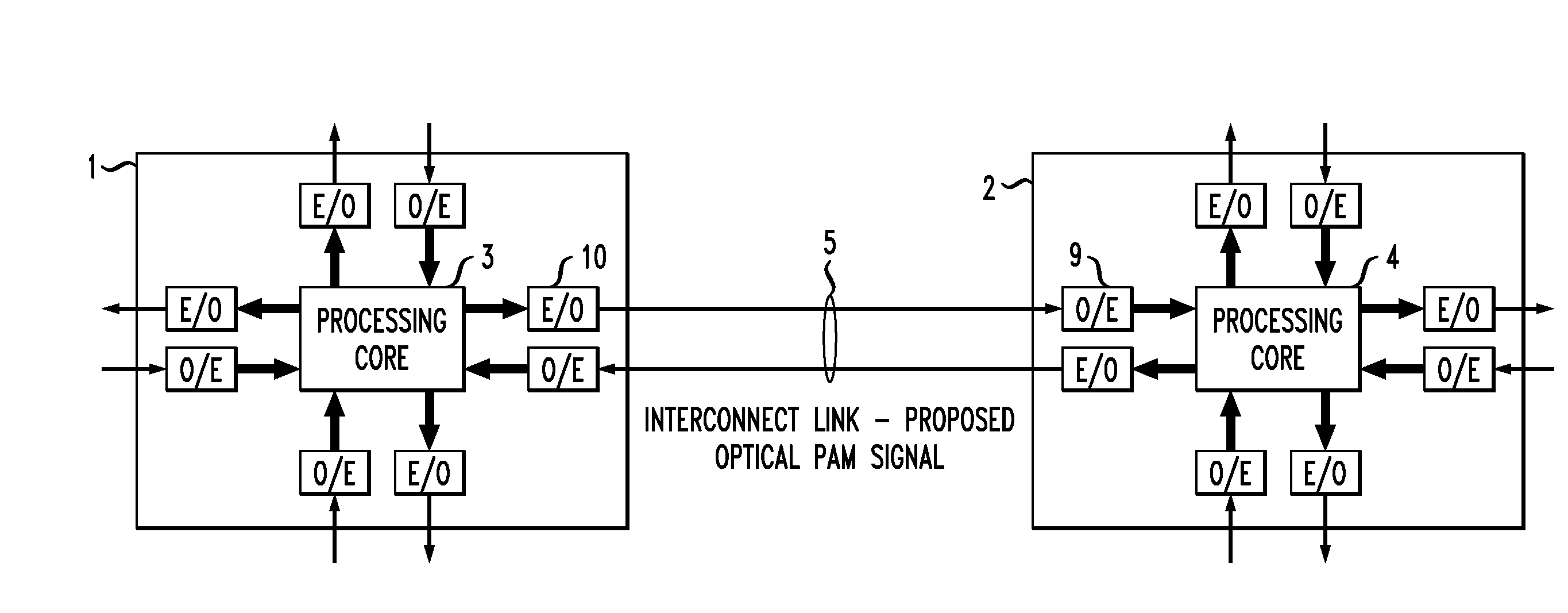
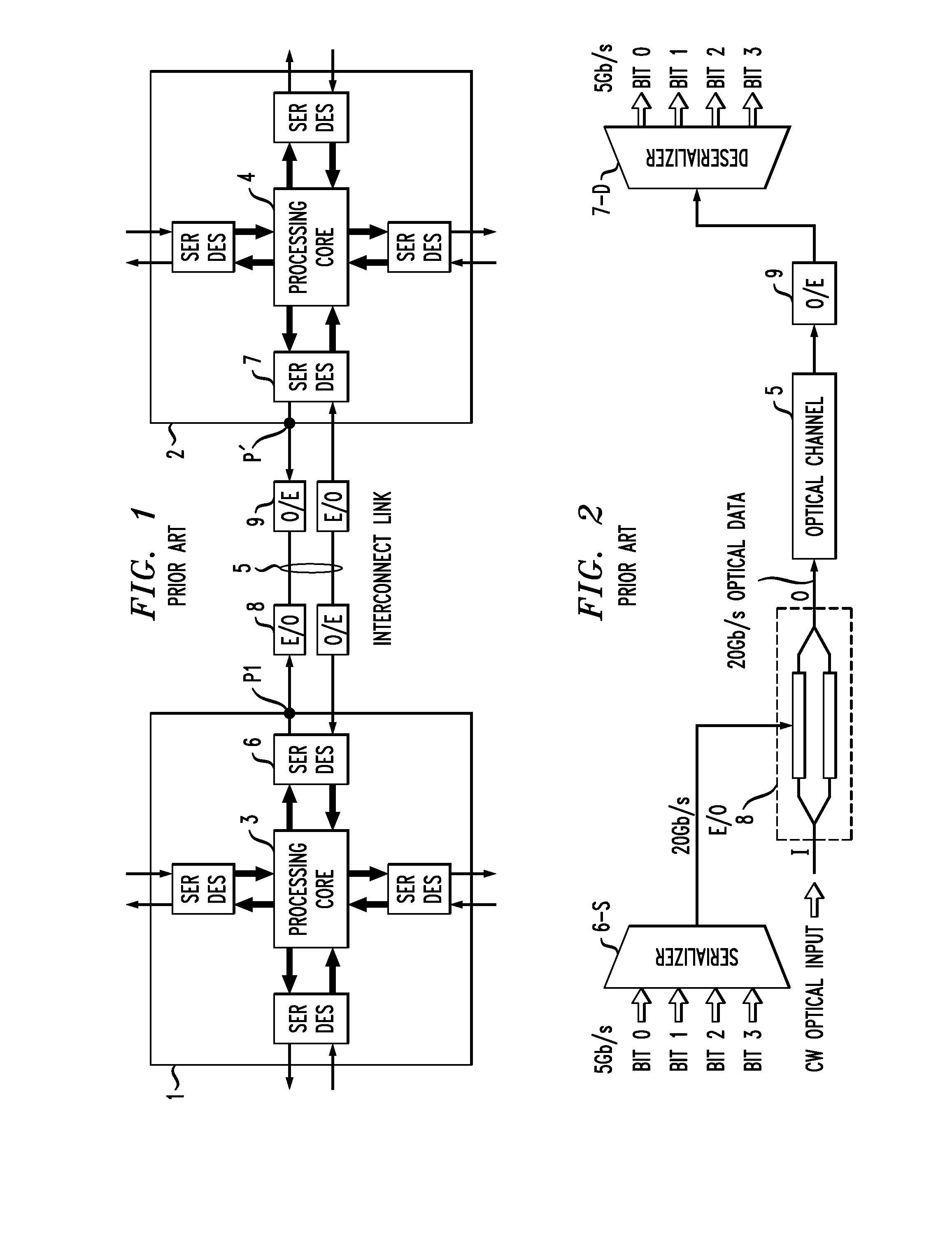
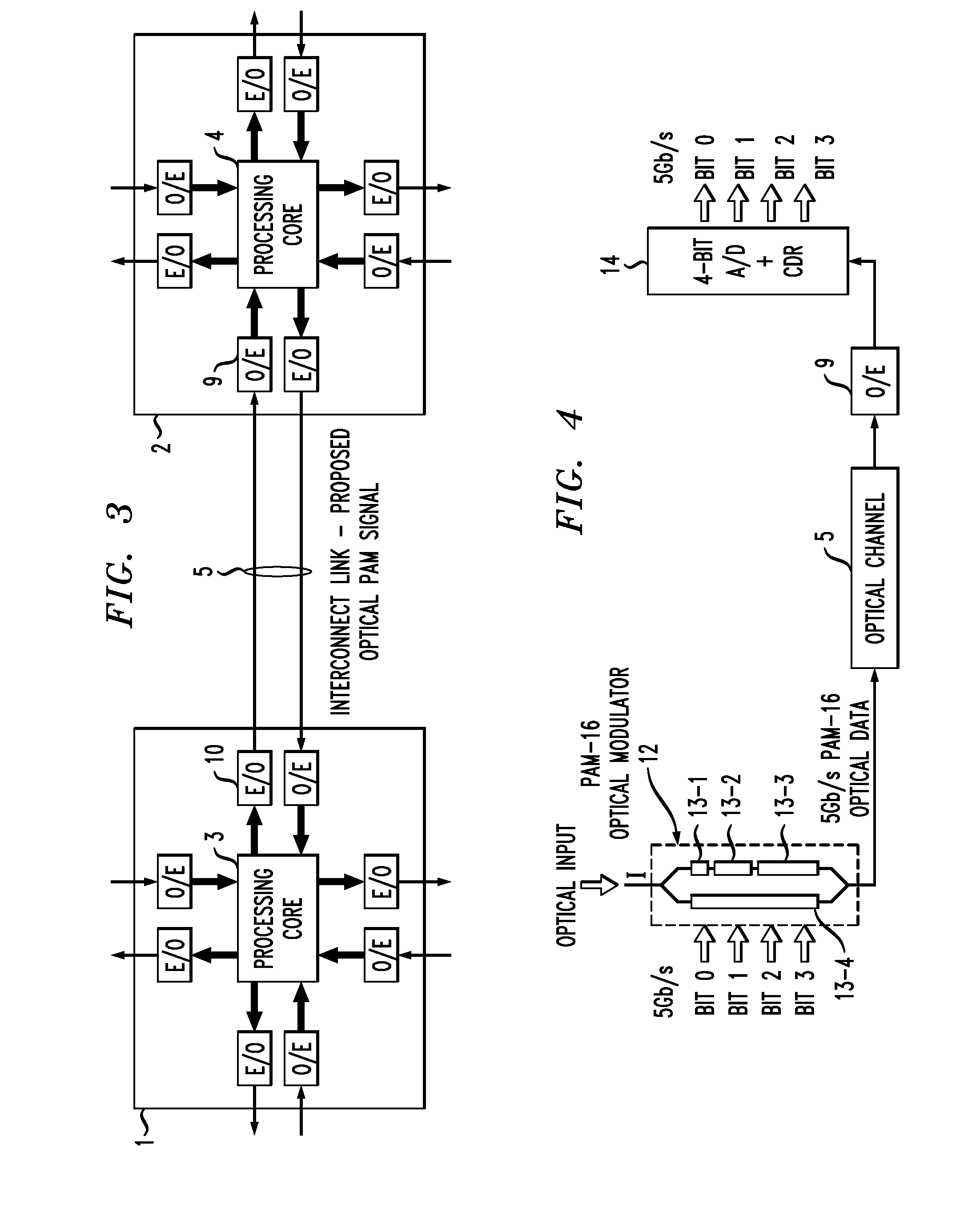
[0022]FIG. 1 illustrates a conventional prior art optical interconnect arrangement between a first chip 1 and a second chip 2. Chip 1 includes a processing core 3 that functions to manipulate massive amounts of data in a parallel word format. A similar processing core 4 is included within chip 2, and there is a need to provide communication between chips 1 and 2 via an optical interconnect link 5. It is to be understood that only a single link 5 is shown for the purposes of clarity. In ...


PUM


Abstract

An optical interconnection arrangement for use in high data applications is presented that eliminates the need for extensive serialization/de-serialization (SERDES) functionality by utilizing pulse amplitude modulation (PAM) techniques to represent the data in the optical domain while utilizing a separate channel for transmitting an optical clock signal, eliminating the need for clock recovery circuitry on the receive end of the arrangement.

Description

CROSS-REFERENCE TO RELATED APPLICATIONS [0001]This application claims the benefit of U.S. Provisional Application No. 61 / 186,718, filed Jun. 12, 2009 and herein incorporated by reference.TECHNICAL FIELD [0002]The present invention relates to an optical interconnection arrangement and, more particularly, to an arrangement that reduces the need for extensive serialization / de-serialization (SERDES) functionality by utilizing pulse amplitude modulation (PAM) techniques in combination with a separate transmission channel for a clock signal.BACKGROUND OF THE INVENTION[0003]Due to the continuing demand for computing and networking applications, there is a growing demand for high performance computing (HPC) platforms, as well as large data centers. In either case, the interconnects between computer servers or network nodes have not been able to keep up with the growth in computing power within the chip or server. The bottlenecks include, but are not limited to, chip-to-chip communication po...

Claims


Application Information

Patent Timeline
Patent Type & Authority Applications(United States)
IPC IPC(8): H04B10/12H04B10/2581
CPCH04B10/801H04L7/0008H04L7/0075H04B10/505H04B10/516H04B10/524H03K7/02H04B10/00H04B10/2581
Inventor SHASTRI, KALPENDUDAMA, BIPINWEBSTER, MARK
Owner CISCO TECH INC
Why Eureka
Try Eureka