
Eureka
For R&D, Eureka makes reading and utilizing patents & technical documents easy.
Eureka AIR
Designed for self-driven R&D workflows. Generate viable solutions, solve complex R&D challenges, empower your innovation with AI.

Eureka Materials
Designed for material experts only. Revolutionize your material R&D, from search, analyze, to developing new materials.

TechResearch
Generate reliable direction feasibility study reports for your R&D in just a few steps.

TechSeek
Discover and master advanced knowledge NOW. Basics, ideas, possibilities, all at once.

TechMind
As an expert in R&D Theories, TechMind can generates customized viable solutions instantly.

TechRisk
Analyze your overall solution with one click, know your potential R&D risks in advance.

TechMonitor
Get weekly tech updates, stay abreast of the latest tech innovations and key insights.
Method of fabricating electron emission source and method of fabricating electronic device by using the method
- Summary
- Abstract
- Description
- Claims
- Application Information
AI Technical Summary
Benefits of technology
Problems solved by technology
Method used
Image

Examples
Embodiment Construction
[0022]The present invention will now be described more fully with reference to the accompanying drawings, in which exemplary embodiments of the invention are shown.
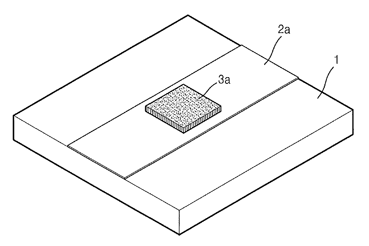
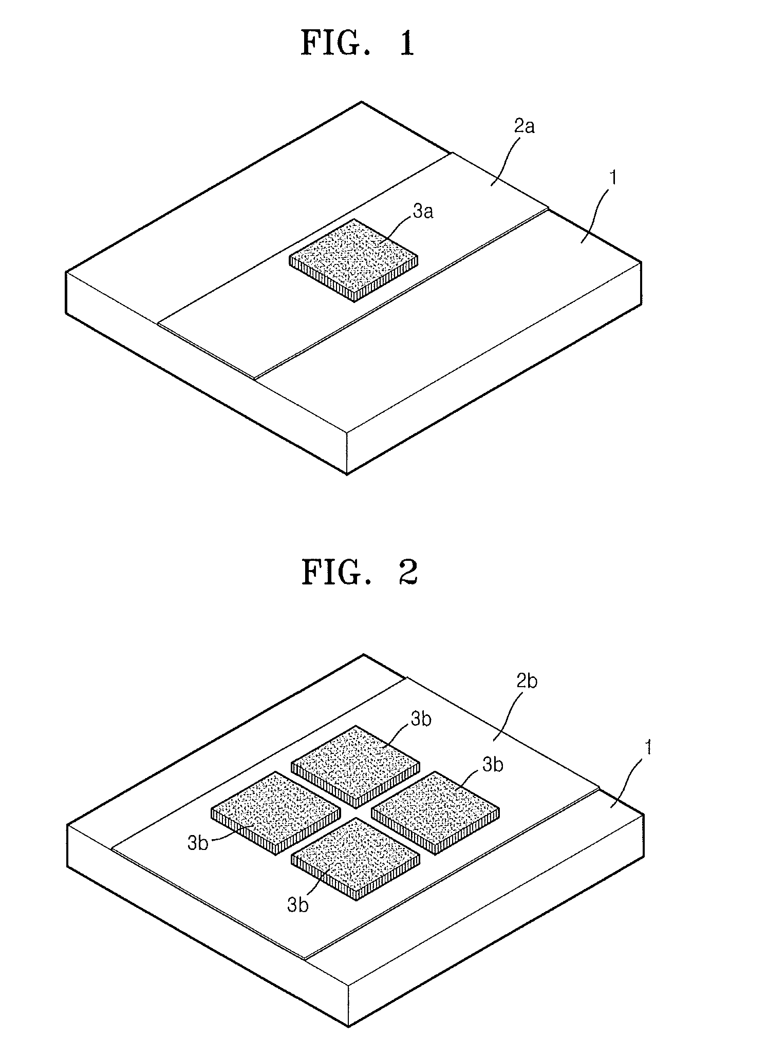
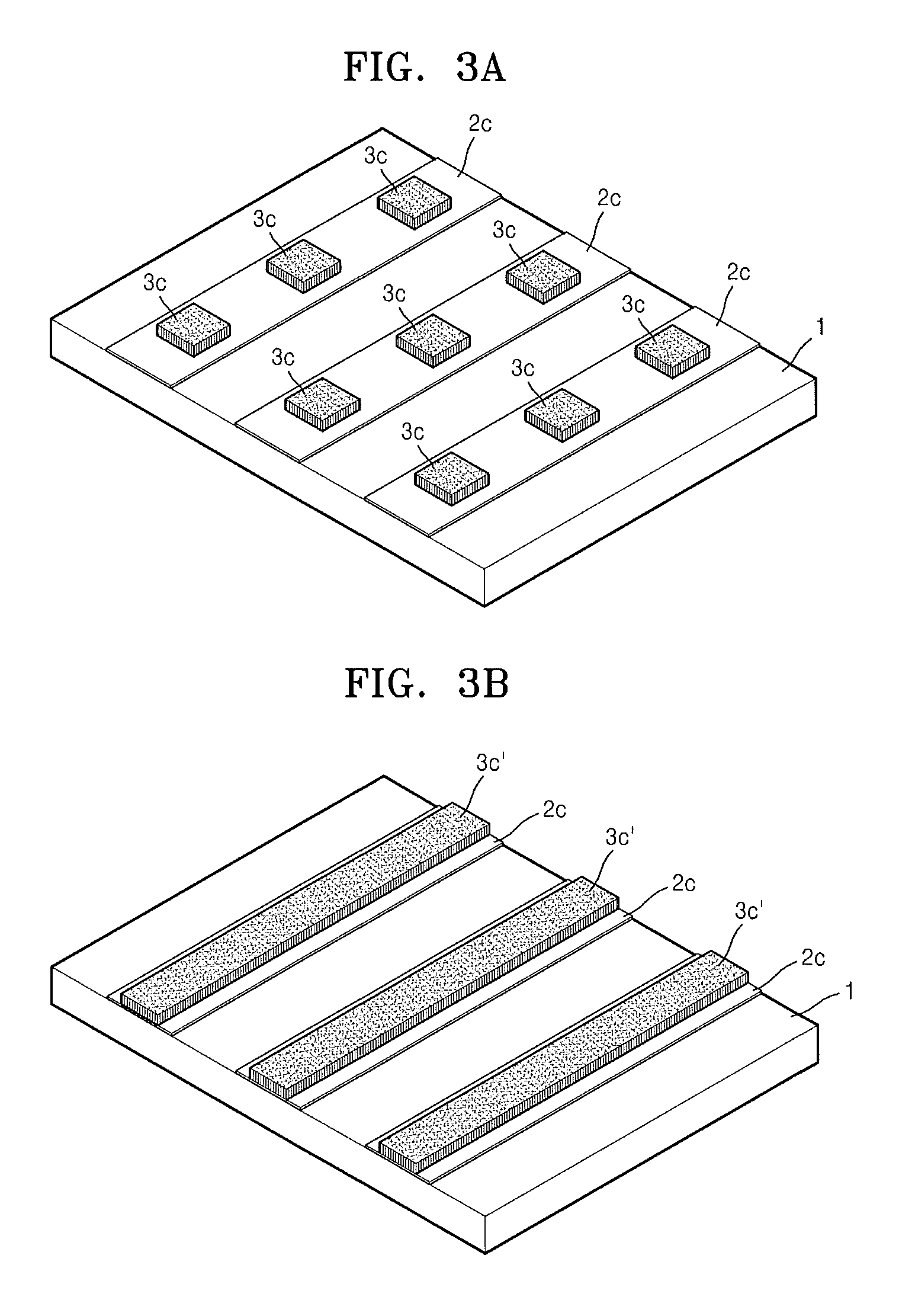
[0023]The present invention uses a needle-shaped electron emission material. The needle-shaped electron emission material may be in the form of hollow nanotubes, non-hollow nanorods, nanowires, fibers, or nanofibers. The needle-shaped electron emission material may be carbon, but may also be other metallic materials. In the following embodiments of the present invention, carbon nanotubes (CNT) will be described as a representative example of the needle-shaped electron emission material. However, all needle-shaped electron emission materials may be used. Thus, the present invention is not limited to a particular example of the needle-shaped electron emission material.
[0024]FIGS. 1, 2, 3A, and 3B are schematic perspective views of electron emission sources according to embodiments of the present invention. Referring to FIG....
PUM
 Abstract
Description
Claims
Application Information
 - R&D Engineer
- R&D Manager
- IP Professional
- Industry Leading Data Capabilities
- Powerful AI technology
- Patent DNA Extraction
Browse by: Latest US Patents, China's latest patents, Technical Efficacy Thesaurus, Application Domain, Technology Topic, Popular Technical Reports.
© 2024 PatSnap. All rights reserved.Legal|Privacy policy|Modern Slavery Act Transparency Statement|Sitemap|About US| Contact US: help@patsnap.com