Method for making microstructured objects

a technology of microstructured objects and methods, applied in the direction of manufacturing tools, electrical-based machining electrodes, transportation and packaging, etc., can solve the problems of microstructure loss, wear off the surface, and difficulty in coating application

Inactive Publication Date: 2010-12-23
HOOWAKI
View PDF4 Cites 49 Cited by
  • Summary
  • Abstract
  • Description
  • Claims
  • Application Information

AI Technical Summary

Benefits of technology

[0015]providing a semiconductor wafer, patterning the semiconductor wafer with said preselected pattern of microfeatures, molding an uncured flexible polymer to the patterned semiconductor wafer, curing the polymer, thereby forming a microstructured flexible polymer having said preselected pattern of microfeatures, removing said microstructured flexible polymer from said patterned semiconductor wafer and deforming at least a portion of said microstructured flexible polymer so as to conform the microstructured flexible polymer to at least a portion of the surface of the one or more macro scale features of said microstructured prototype. Fabricating said microstructured prototype can include the steps deforming at least a portion of the microstructured polymer is deformed to radius of curvature selected over the range of 100 μm to 3 m and can include deforming at least a portion of said microstructured polymer is deformed to a strain level selected over the range of 1% to 1300%. The semiconductor wafer can be patterning said semiconductor wafer using a method selected from the group consisting of: photolithography, laser ablation, e-beam lithography, nano-imprint lithography and any combination of these.

Problems solved by technology

However, historically, these microfeatures were applied to surfaces as coating or adhesives and therefore are prone to wear off the surface.
Over time the properties provided by the microstructures are lost given the peeling or premature removal of the coating.
Further, the coating can be difficult to apply consistent to curved surfaces and in applications such as molds or other industrial uses, can quickly wear aware from the manufacturing tool.

Method used


Image

  • Method for making microstructured objects
  • Method for making microstructured objects
  • Method for making microstructured objects

Examples


example 1

Microstructure Forming Process Chain and Process Details

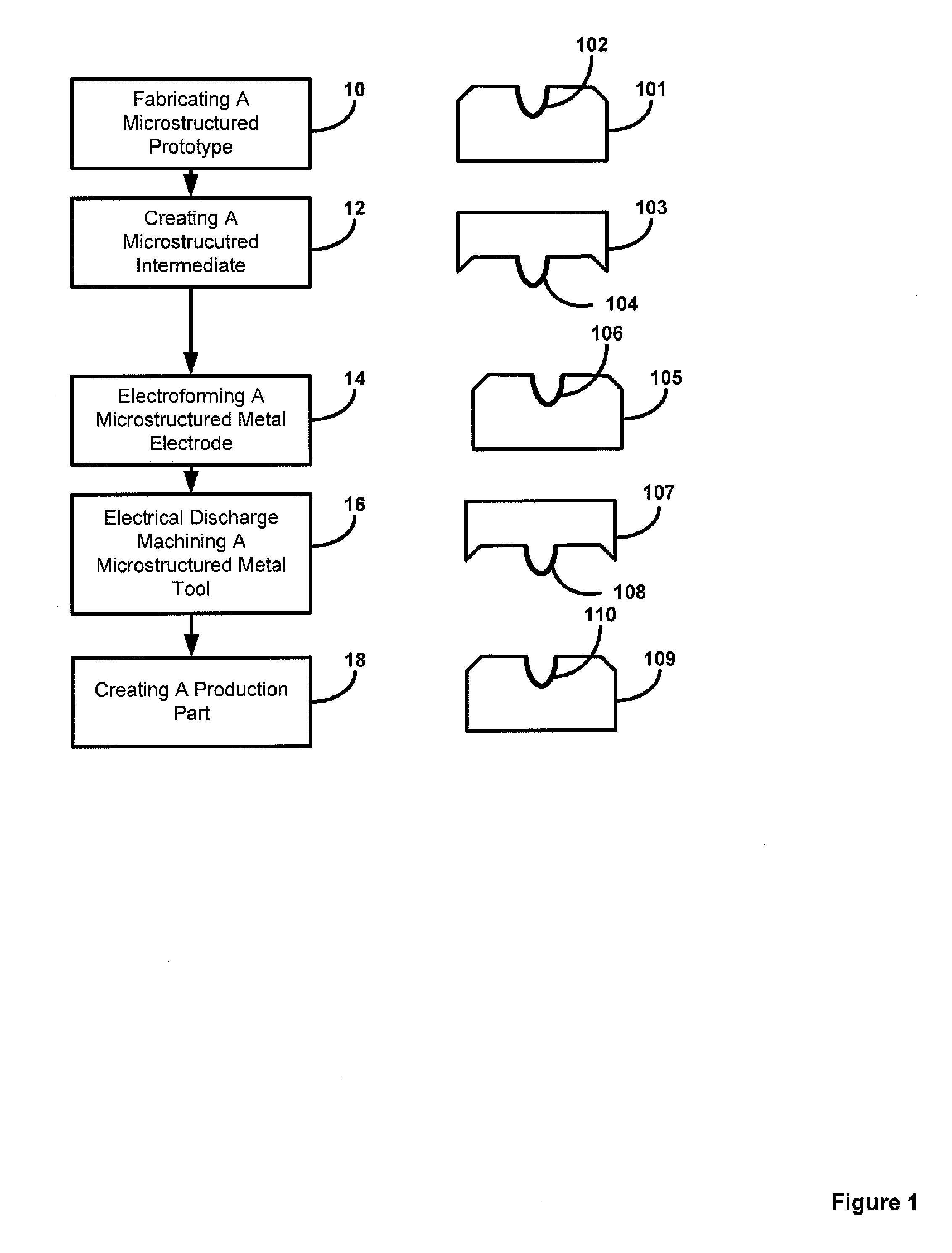
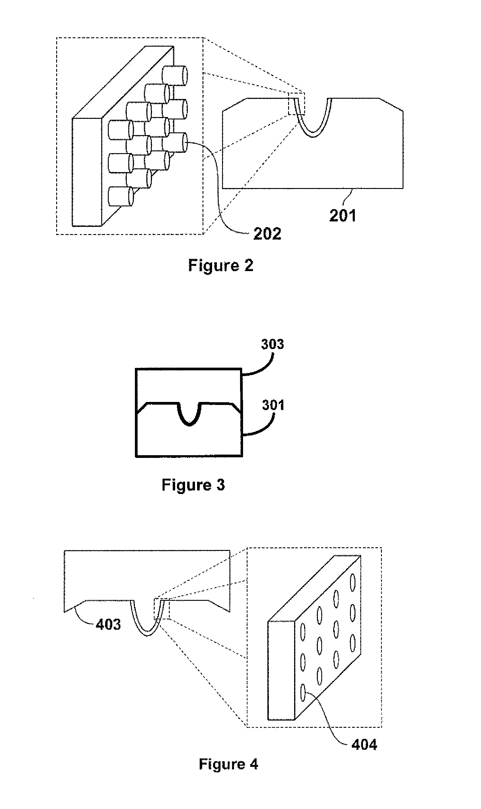
[0071]This example describes a method of generating microstructures into the curved surfaces of two different material classes: rubber and metal. In this embodiment, the creation process begins with a prototype that has microstructures incorporated into its curved surface. An intermediate, rubber in one embodiment, is carried by a curved surface of the microstructured prototype, a metal electrode is generated through electroforming on the curved surface of the microstructured prototype. However, the metal electrode could be created using metal injection molding and / or embossing. A metal tool is then generated from the metal electrode. In one embodiment, the metal electrode is used to electrical discharge machine a metal tool resulting in a microstructured curved metal mold surface that can be used for the production part. The microstructures replicate through the steps of the process chain.

[0072]While this example describes the...

example 2

Fabrication Method for Tailored Micrometer-Scale and Nanometer-Scale Structures

[0075]In one embodiment, fabricating Lithographically Defined Arrays of Micro / Nanostructures (LDAMN) can be used. The technique begins with a substrate topped with a photosensitive polymer or resist sensitive to light or particles. By shining light through a stencil mask onto the resist, micrometer-scale or nanometer-scale structures can be formed in the resist. Other kinds of electromagnetic waves, energy beams, or particles can also be used to form these microstructures or nanostructures. The structures can be arrayed into patterns or not, but their key characteristic is that the manufacturing process controls their size, shape, and position with micrometer-scale or nanometer-scale accuracy and precision.

[0076]The resist having tailored microstructures or nanostructures can be used as a mold at this stage. The substrate can also be treated (for example with a chemical etch) to modify the microstructures...

example 3

Reusability of Microstructured Objects and Heterogeneity of Microfeatures

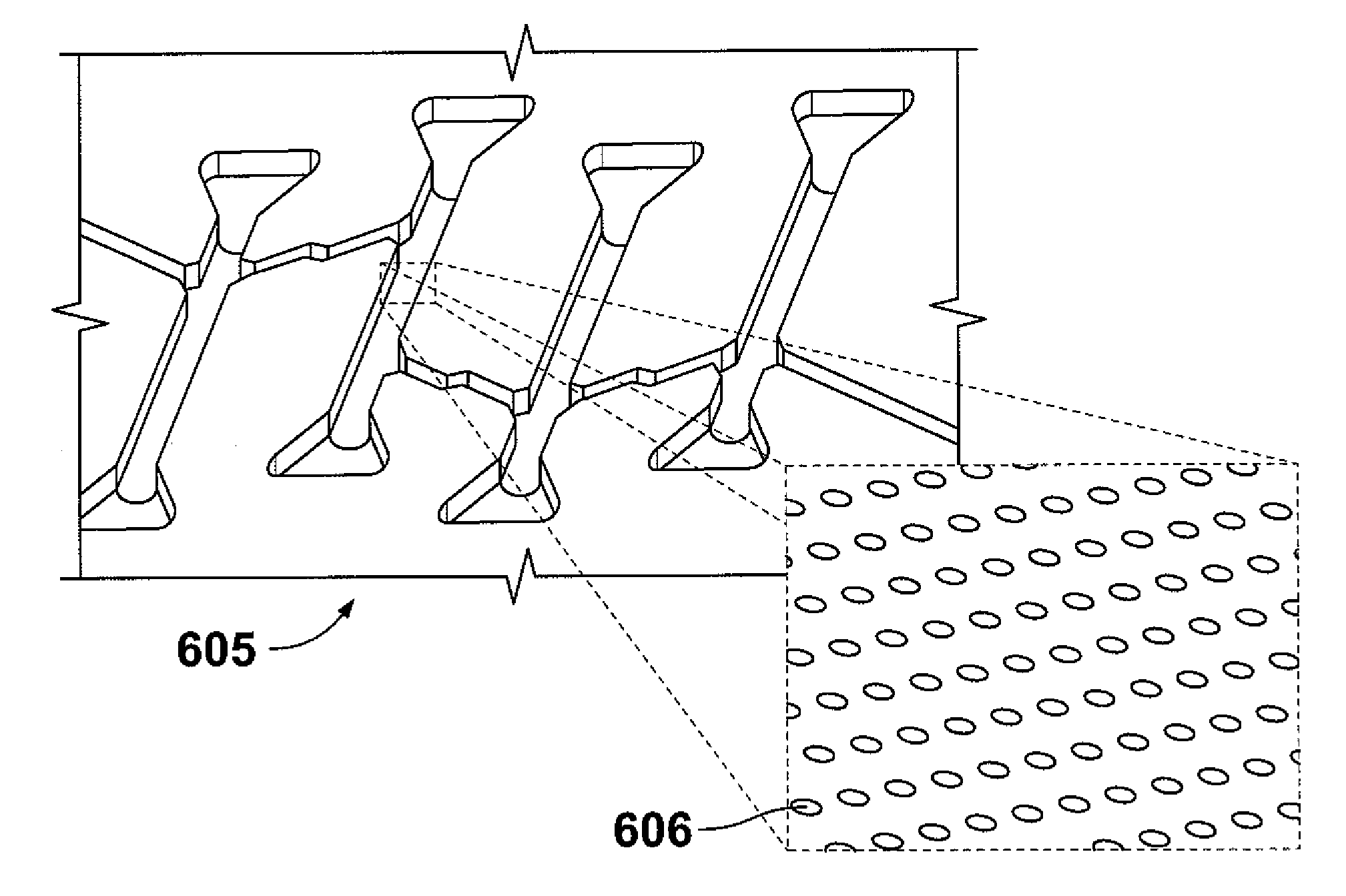
[0079]A microstructured prototype having a preselected pattern of microfeatures can be fabricated in this example. In this embodiment, the preselected pattern included two regions of different microfeature shapes. The first region included micropillars 100 μm tall with 100 μm wide triangular cross-sectional shapes. The second region included micropillars 100 μm tall with 100 μm wide circular cross-sectional shapes.

[0080]An intermediate can be cast to the microstructured prototype to create a first microstructured intermediate object. The microstructured intermediate object thus produced included the two regions of different microfeature shapes formed from the casting of those of the microstructured prototype. The first region formed microholes 100 μm deep with 100 μm wide triangular cross-sectional shapes in the microstructured rubber. The second region formed microholes 100 μm deep with 100 μm wide circular cr...


PUM

PropertyMeasurementUnit
thicknessaaaaaaaaaa
thicknessaaaaaaaaaa
thicknessaaaaaaaaaa

Abstract

Described herein are casting and molding methods useful for making microstructured objects. By including a plurality of microfeatures on the surface of an object, other characteristics may be imparted to the object, such as increased hydrophobicity. Some of the casting and molding methods described herein further allow for manufacture of objects having both microfeatures and macro features, for example microfeatures on or within macro features or selected macro feature regions.

Description

CLAIM OF PRIORITY[0001]This application claims the benefit of and priority of PCT Patent Application: US09 / 43306, “Method of Manufacturing Microstructures”, filed on May 8, 2009; PCT Patent Applications: US09 / 43307, “Flexible Microstructured Superhydrophobic Materials”, filed on May 8, 2009 and PCT Patent Application: US09 / 49565, “Casting Microstructures into Stiff and Durable Materials from a Flexible and Reusable Mold”, filed on Jul. 2, 2009 incorporated by reference and pursuant to 35 U.S.C. §111.FIELD OF THE INVENTION[0002]This invention is in the field of electroforming and electrical discharge machining (EDM) methods. This invention relates generally to methods of making microstructured objects by electroforming and by electrical discharge machining.BACKGROUND OF THE INVENTION[0003]Microfeatures placed on an object can provide for advantageous surface properties for such an object. By including a plurality of microfeatures on the surface of an object, other characteristics may...

Claims


Application Information

Patent Timeline
Patent Type & Authority Applications(United States)
IPC IPC(8): B23H7/22
CPCB23H1/06B23H9/00Y10T428/24702Y10T29/49002Y10T29/49144Y10T29/49121Y10T428/24Y10T29/49117Y10T29/49204
Inventor HULSEMAN, RALPH A.MAMMARELLA, ROBERT E.MAGUIRE, MARCH
Owner HOOWAKI
Why Eureka
Try Eureka