Digital radiography imager with buried interconnect layer in silicon-on-glass and method of fabricating same

a radiography imager and interconnect layer technology, applied in the field of imaging arrays, can solve the problems of addressing and readingout interconnect, low light collection efficiency, and high resistance power of the lenslett, and achieve the effects of reducing the cost of addressing and readingout, and improving light collection efficiency

Inactive Publication Date: 2010-12-23
CARESTREAM HEALTH INC
View PDF12 Cites 129 Cited by
  • Summary
  • Abstract
  • Description
  • Claims
  • Application Information

AI Technical Summary

Benefits of technology

[0009]In another aspect, the present invention provides an imaging array. The imaging array includes a glass substrate, a single crystal silicon layer having a thickness of less than about 5 microns, an electrically conductive layer, first conductive areas, and an array of photosensitive elements. The single crystal silicon layer is secured to the glass substrate. The electrically co

Problems solved by technology

Lensletts do not provide any improvement in light collection efficiency for imaging arrays in contact with a scintillator.
In addition, because of the need to maximize f

Method used


Image

  • Digital radiography imager with buried interconnect layer in silicon-on-glass and method of fabricating same
  • Digital radiography imager with buried interconnect layer in silicon-on-glass and method of fabricating same
  • Digital radiography imager with buried interconnect layer in silicon-on-glass and method of fabricating same

Examples


Embodiment Construction

[0015]As noted above, the present invention relates to an improved image sensing device and a method of making such a device. The device preferably is a large area, e.g., approximately greater than 6 inches by 6 inches, flat panel digital radiography imaging sensor. The invention is not limited to this application, however, as the methodologies described below could be used in other applications. Preferred embodiments of the invention now will be described with reference to the Figures.

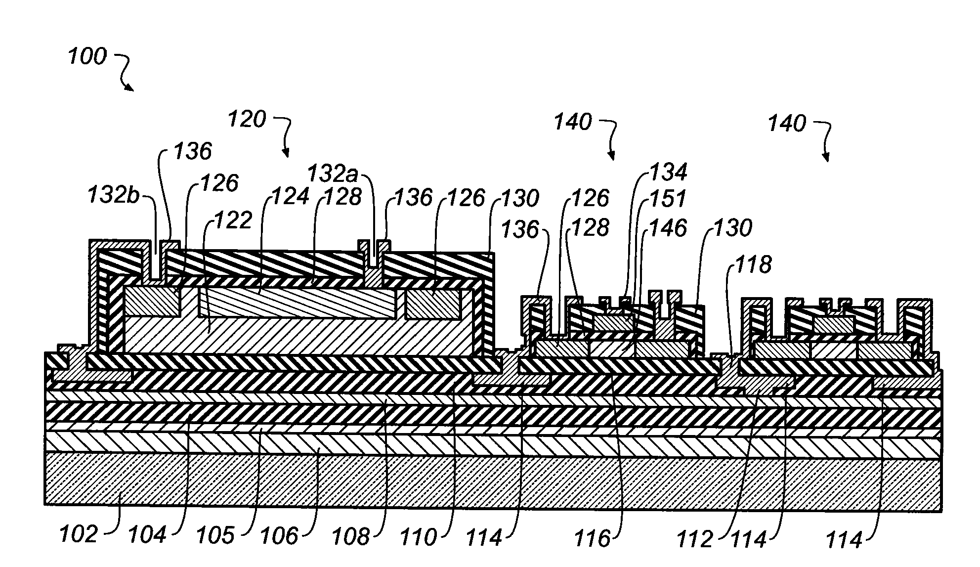
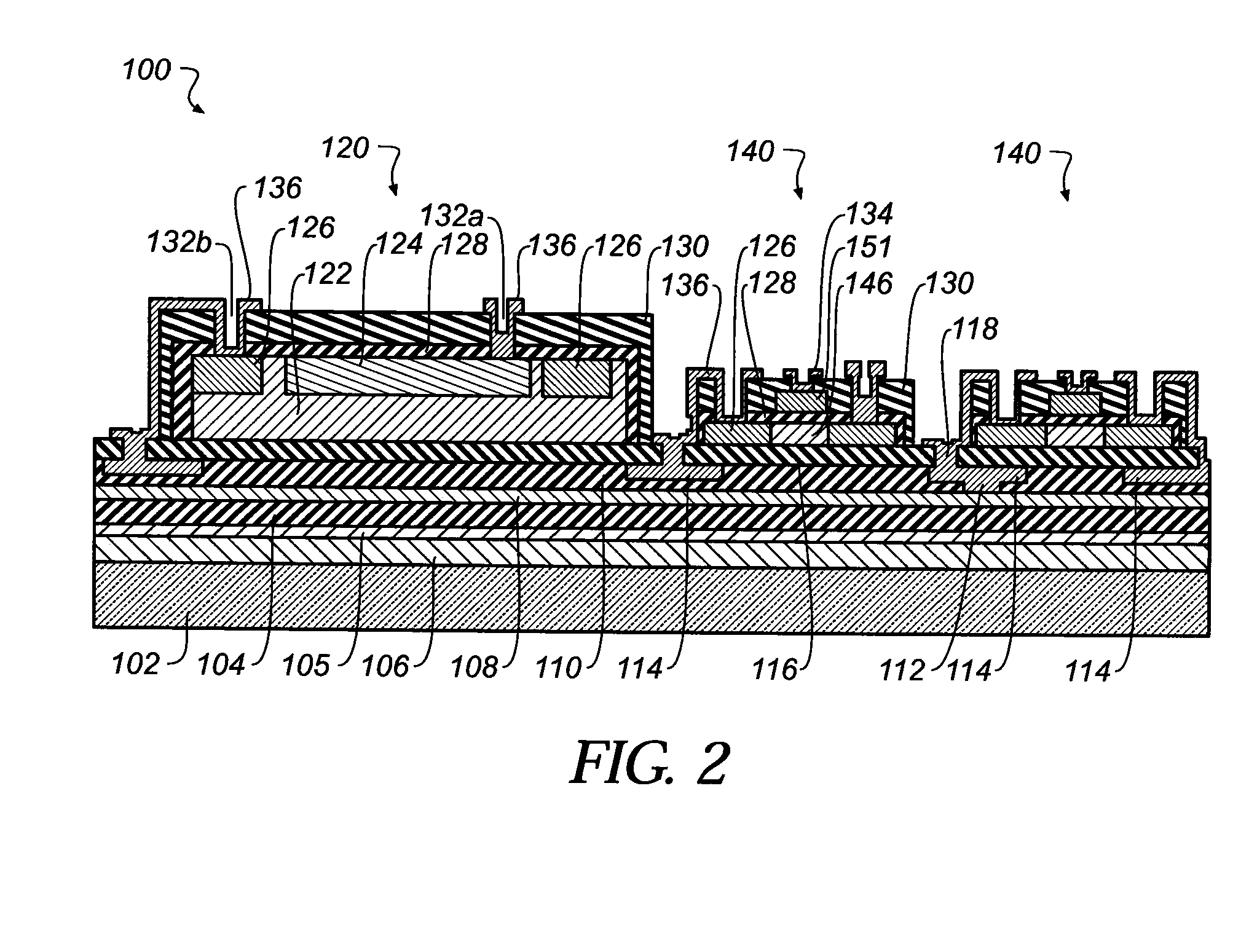
[0016]FIG. 2 is a cross-sectional view of a pixel 100 according to a preferred embodiment of the invention. The pixel 100 is one of multiple pixels in an array and is formed on a glass substrate 102 to which a silicon layer 105 is bonded via an anodic bond 106. A first insulating layer 104, which is a dielectric, preferably formed from an inorganic insulating material such as silicon dioxide, is disposed on the silicon layer 105. A first patterned conductive layer 108 is disposed on the first insulati...


PUM


Abstract

A method of forming an imaging array includes providing a single crystal silicon substrate having an internal separation layer, forming a patterned conductive layer proximate a first side of the single crystal silicon substrate, forming an electrically conductive layer on the first side of the single crystal silicon substrate and in communication with the patterned conductive layer, securing the single crystal silicon substrate having the patterned conductive layer and electrically conductive layer formed thereon to a glass substrate with the first side of the single crystal silicon substrate proximate the glass substrate, separating the single crystal silicon substrate at the internal separation layer to create an exposed surface opposite the first side of the single crystal silicon substrate and forming an array comprising a plurality of photosensitive elements and readout elements on the exposed surface.

Description

TECHNICAL FIELD[0001]The present invention relates to imaging arrays on insulating substrates. More specifically, the invention relates to an imaging array for use in a large area flat panel digital radiography imaging sensor formed using silicon on glass and having one or more buried interconnect layers formed on the silicon wafer prior to being attached to the glass substrate.DESCRIPTION OF RELATED ART[0002]Image sensors fabricated in single-crystal silicon and from deposited semiconductors, such as amorphous or polycrystalline silicon, are well known.[0003]Image sensor arrays fabricated in single-crystal silicon generally include a photosensitive element, a readout circuit and several layers of metal interconnect. Examples of photosensitive elements include p-n junction photodiodes, metal-insulator-semiconductor photo-capacitors, charge coupled devices, phototransistors, and pinned photodiodes. Examples of readout circuits include charge-coupled devices, passive pixel readout cir...

Claims


Application Information

Patent Timeline
IPC IPC(8): H01L31/00H01L31/10
CPCH01L27/14609H01L27/14692H01L27/14689
Inventor TREDWELL, TIMOTHY J.LAI, JACKSON
Owner CARESTREAM HEALTH INC
Why Eureka
Try Eureka