Semiconductor device and manufacturing method thereof

a semiconductor device and manufacturing method technology, applied in the direction of transistors, basic electric elements, electric devices, etc., can solve the problems of reducing the throughput of a semiconductor device or increasing the manufacturing cost and achieve the effect of improving the performance of a semiconductor devi

Inactive Publication Date: 2010-12-23
RENESAS ELECTRONICS CORP
View PDF7 Cites 9 Cited by
  • Summary
  • Abstract
  • Description
  • Claims
  • Application Information

AI Technical Summary

Benefits of technology

[0015]It is therefore effective to select different insulating materials for the gate insulating film of the n-channel MISFET and the gate insulating film of the p-channel MISFET in order to independently control the threshold voltages of the n-channel MISFET and p-channel MISFET.
[0016]As a high dielectric constant film (high-k film) for a gate insulating film, an Hf-based gate insulating film which is a high dielectric constant film containing Hf is excellent. Introduction of a rare earth element (particularly preferably, lanthanum) into the Hf-based gate insulating film of the re-channel MISFET can reduce the threshold value of the n-channel MISFET. Introduction of aluminum into the Hf-based gate insulating film of the p-channel MISFET can, on the other hand, reduce the threshold value of the p-channel MISFET. It is therefore possible to reduce both of the threshold values of the n-channel MISFET and the p-channel MISFET by selectively introducing a rare earth element (particularly, lanthanum) into the Hf-based gate insulating film of the n-channel MISFET and selectively introducing aluminum into the Hf-based gate insulating film of the p-channel MISFET.
[0018]Since an Hf-based gate insulating film containing no Si such as an HfON film has a higher dielectric constant than an Hf-based gate insulating film containing Si such as an HfSiON film, use of an Hf-based gate insulating film containing no Si is effective in order to reduce the EOT of the Hf-based gate insulating film. The investigation by the present inventors has however revealed that when a rare earth element such as La is introduced into an Hf-based gate insulating film containing no Si to convert it into an HfLaON film, there is a risk of inconvenience due to a weak binding power between La and Hf. For example, upon dry etching for processing a gate electrode or wet etching of a gate insulating film not covered with a gate electrode which will be conducted later, there is a risk of inconvenience such as generation of a foreign matter or retreat of the HfLaON film, which is a gate insulating film, from the side surface of the gate electrode due to easy separation or elution of LaO from the HfLaON film. This may deteriorate the performance of the resulting semiconductor device. In addition, for the reduction of a threshold value by introducing La into the Hf-based gate insulating film of an n-channel MISFET, La is preferably diffused sufficiently in the Hf-based gate insulating film in a substrate direction. In the HfLaON film, compared with in the HfLaSiON film, La is not diffused easily due to a weak binding power between La and Hf. A threshold value reducing effect produced by introduction of La is therefore smaller in the n-channel MISFET using an HfLaON film as the gate insulating film than in the n-channel MISFET using an HfLaSiON film as the gate insulating film. As a result, an absolute value of the threshold voltage becomes greater. This also deteriorates the performance of the semiconductor device.
[0019]An object of the present invention is to provide a technology capable of improving the performance of a semiconductor device equipped with a CMISFET having a high dielectric constant gate insulating film and a metal gate electrode.
[0026]The typical embodiment of the invention enables to improve the performance of a semiconductor device.

Problems solved by technology

Using different materials for the metal gate electrode of the n-channel MISFET and the metal gate electrode of the p-channel MISFET makes a manufacturing step (gate electrode forming step) of a semiconductor device cumbersome and complicated and causes a decrease in throughput of a semiconductor device or an increase in the manufacturing cost of the semiconductor device.

Method used


Image

  • Semiconductor device and manufacturing method thereof
  • Semiconductor device and manufacturing method thereof
  • Semiconductor device and manufacturing method thereof

Examples


embodiment 1

[0062]The semiconductor device according to the present embodiment will next be described based on some drawings.

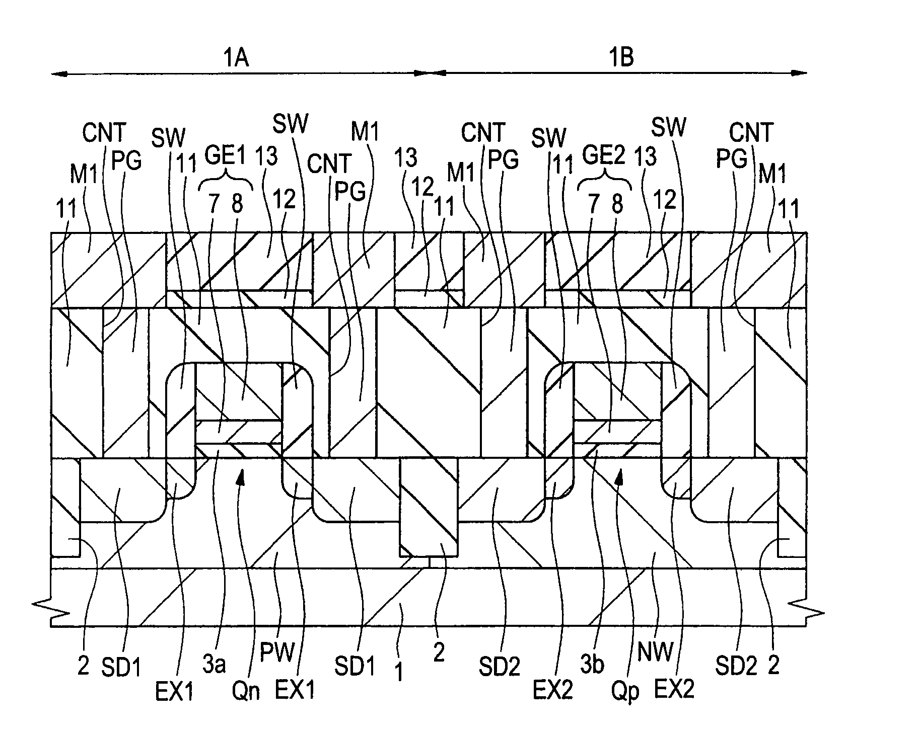
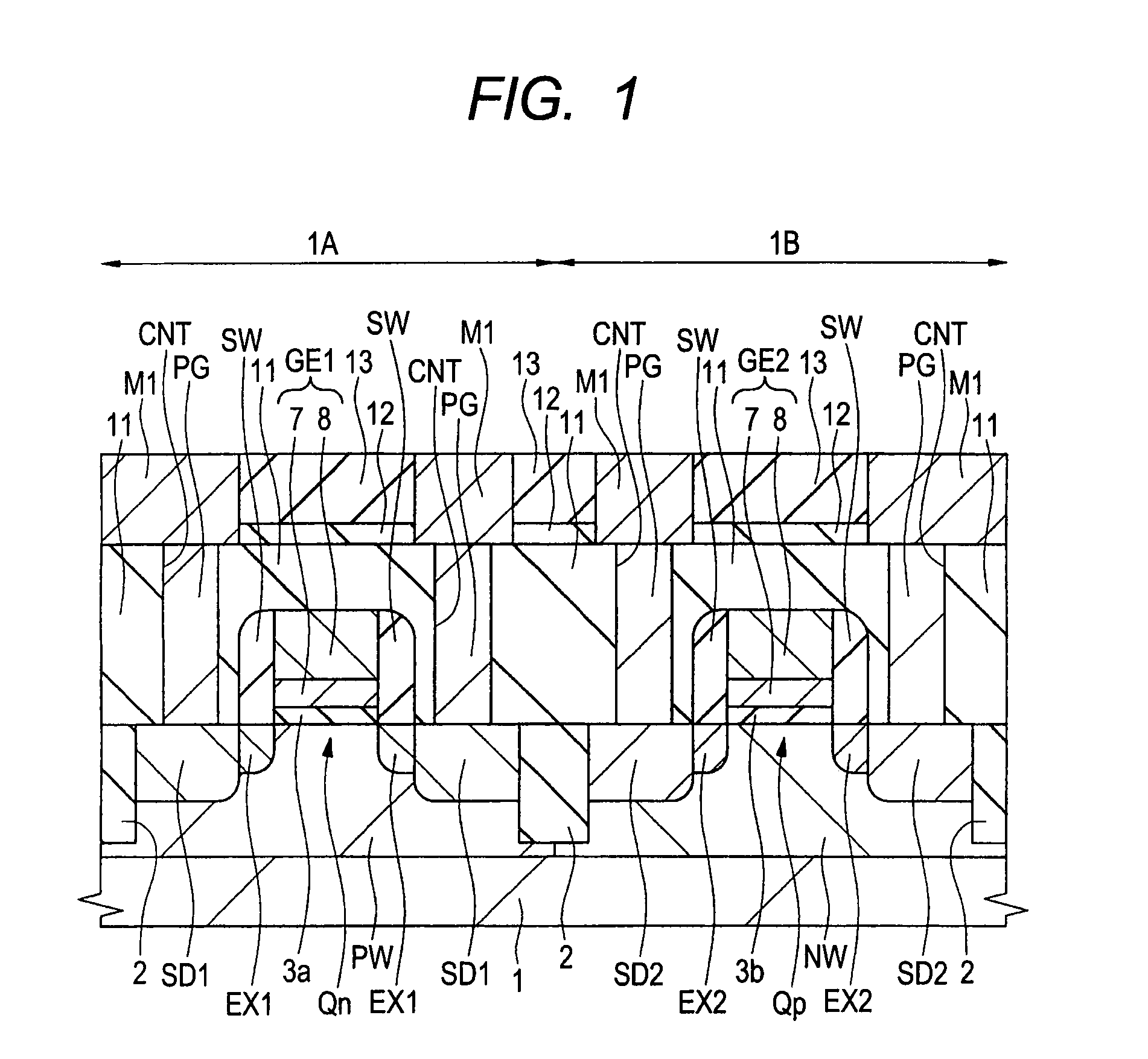
[0063]FIG. 1 is a fragmentary cross-sectional view of a semiconductor device according to one embodiment of the invention, that is, a semiconductor device having a CMISFET (complementary metal insulator semiconductor field effect transistor).

[0064]As illustrated in FIG. 1, the semiconductor device according to the present embodiment has an n-channel MISFET (metal insulator semiconductor field effect transistor: MIS field effect transistor) Qn formed in an nMIS formation region 1A of a semiconductor substrate 1 and a p-channel MISFET Qp formed in a pMIS formation region 1B of the semiconductor substrate 1.

[0065]Described specifically, the semiconductor substrate 1 comprised of, for example, a p type single crystal silicon has an nMIS formation region (first region) 1A and a pMIS formation region (second region) 1B which are electrically isolated from each other, defined by...

embodiment 2

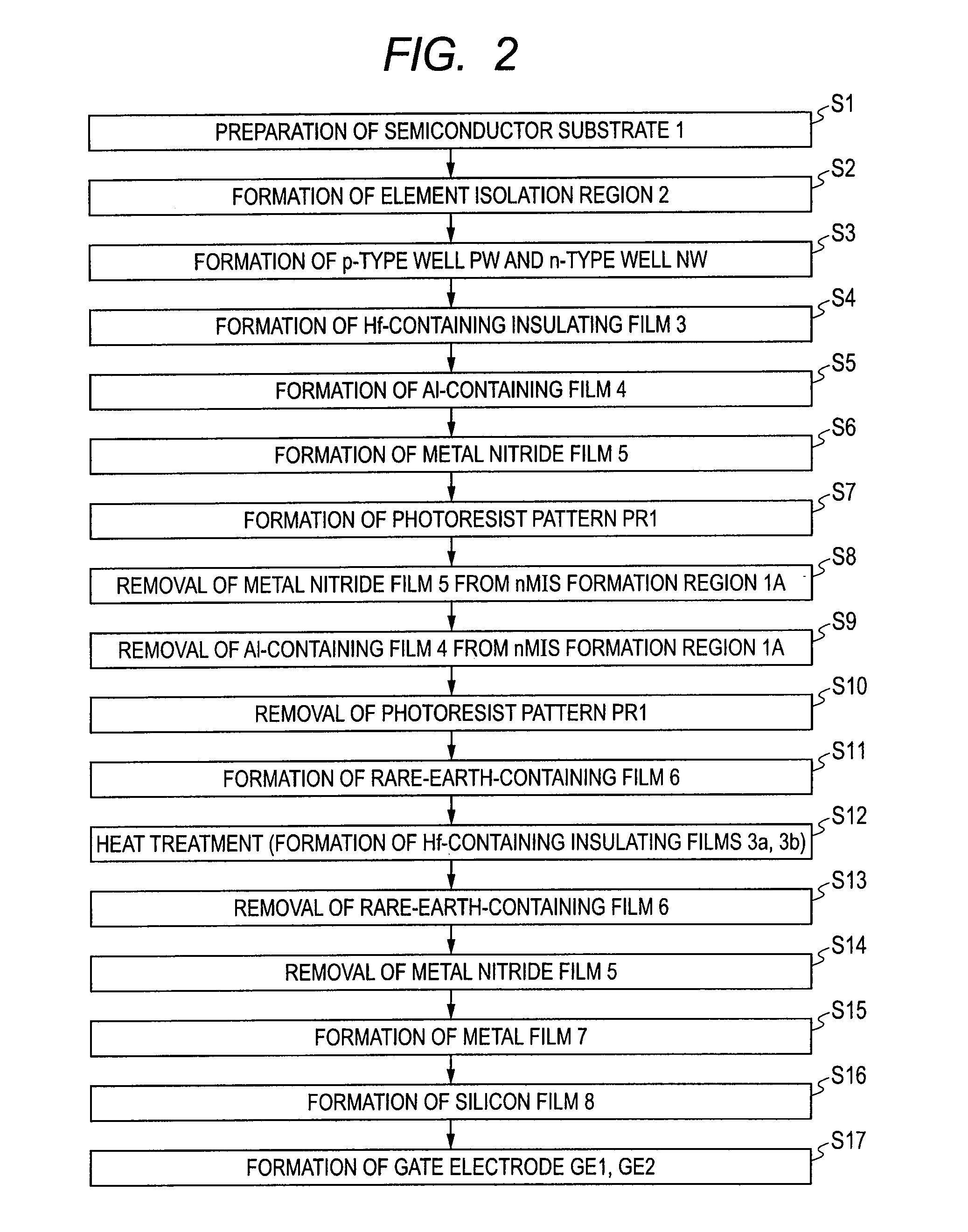
[0172]FIG. 19 is a manufacturing process flow chart showing some manufacturing steps of the present embodiment and corresponds to FIG. 1 of Embodiment 1. FIGS. 20 to 25 are fragmentary cross-sectional view of a semiconductor device of the present embodiment during manufacturing steps thereof. To simplify the chart, Steps S2 to Steps S9 are omitted from FIG. 19.

[0173]The manufacturing steps of the present embodiment until removal of the photoresist pattern PR1 in Step S10 are similar to those of Embodiment 1. Description on them are therefore omitted and steps after Step S10, that is, steps after removal of the photoresist pattern PR1 in Step S10 will next be described.

[0174]After formation of the structure illustrated in FIG. 8 by carrying out similar steps to Steps S1 to S10 of Embodiment 1, a silicon film (silicon layer) 21 is formed as a silicon-containing layer (a layer containing Si) over the main surface of the semiconductor substrate 1 as illustrated in FIG. 20 (Step S11a of ...

embodiment 3

[0196]FIG. 26 is a manufacturing process flow chart showing some manufacturing steps of the present embodiment and it corresponds to FIG. 1 of Embodiment 1. FIGS. 27 to 32 are fragmentary cross-sectional views illustrating a semiconductor device of the present embodiment during the manufacturing steps thereof.

[0197]The manufacturing steps of the present embodiment until removal of the photoresist pattern PR1 in Step S10 are similar to those of Embodiment 1. Description on them are therefore omitted and steps after Step S10, that is, steps after removal of the photoresist pattern PR1 in step S10 will next be described.

[0198]After formation of the structure illustrated in FIG. 8 by the steps similar to Steps S1 to S10 in Embodiment 1, a silicon oxide film (silicon oxide layer) 22 is formed as a silicon-containing layer (a layer containing silicon) over the main surface of the semiconductor substrate 1 as illustrated in FIG. 27 (Step S11c of FIG. 26).

[0199]In the etching step in Steps ...


PUM


Abstract

To improve the performance of a CMISFET having a high-k gate insulating film and a metal gate electrode. An n-channel MISFET has, over the surface of a p-type well of a semiconductor substrate, a gate electrode formed via a first Hf-containing insulating film serving as a gate insulating film, while a p-channel MISFET has, over the surface of an n-type well, another gate electrode formed via a second Hf-containing insulating film serving as a gate insulating film. These gate electrodes have a stack structure of a metal film and a silicon film thereover. The first Hf-containing insulating film is an insulating material film comprised of Hf, a rare earth element, Si, O, and N or comprised of Hf, a rare earth element, Si, and O, while the second Hf-containing insulating film is an insulating material film comprised of Hf, Al, O, and N or comprised of Hf, Al, and O.

Description

CROSS-REFERENCE TO RELATED APPLICATIONS[0001]The disclosure of Japanese Patent Application No. 2009-144512 filed on Jun. 17, 2009 including the specification, drawings and abstract is incorporated herein by reference in its entirety.BACKGROUND OF THE INVENTION[0002]The present invention relates to a semiconductor device and a manufacturing method thereof, particularly to a technology effective when applied to a semiconductor device equipped with a CMISFET having a high-dielectric-constant gate insulating film and a metal gate electrode and a manufacturing method of the semiconductor device.[0003]A MISFET (metal insulator semiconductor field effect transistor) can be formed by forming a gate insulating film over a semiconductor substrate, forming a gate electrode over the gate insulating film, and forming source / drain regions by ion implantation or the like.[0004]In a CMISFET (complementary MISFET), in order to reduce the threshold voltage of both an n-channel MISFET and a p-channel ...

Claims


Application Information

Patent Timeline
Patent Type & Authority Applications(United States)
IPC IPC(8): H01L27/092H01L21/8238
CPCH01L27/092H01L21/823857
Inventor KAWAHARA, TAKAAKISAKASHITA, SHINSUKEKADOSHIMA, MASARU
Owner RENESAS ELECTRONICS CORP
Why Eureka
Try Eureka