
Semiconductor memory device and method for fabricating the same

a memory device and semiconductor technology, applied in semiconductor devices, diodes, electrical devices, etc., can solve the problems of parasitic capacitance increase, degrade the operational reliability degrade the refresh characteristics of a semiconductor memory device, etc., and achieve the effect of reducing the occurrence of gidl and increasing the channel length

Inactive Publication Date: 2010-12-30
SK HYNIX INC
View PDF5 Cites 18 Cited by
  • Summary
  • Abstract
  • Description
  • Claims
  • Application Information

AI Technical Summary

Benefits of technology

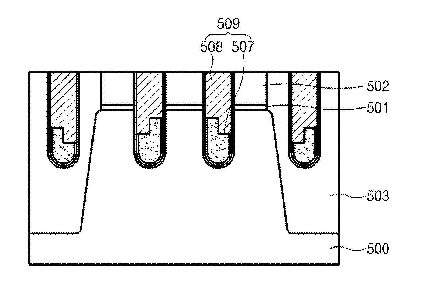
The present invention provides a semiconductor memory device with a buried gate structure and a method for fabricating the same. The method includes etching a predetermined region of a semiconductor substrate to form an isolation layer, depositing a metal layer filling the recess, and asymmetrically etching the metal layer to form an asymmetric gate with a stepped top surface. The asymmetric gate has a reduced occurrence of GIDL and increased channel length. The semiconductor memory device with the buried gate structure includes the asymmetric gate and a capping oxide layer filling the remaining portion of the recess. The asymmetric gate has a predetermined slope and is formed using a tapered etch process. The invention improves the performance and reliability of semiconductor memory devices.

Problems solved by technology

As a result, a channel length becomes shorter, causing a short channel effect and a drain induced barrier lowering (DIBL) effect which may degrade the operational reliability of a semiconductor memory device.
In sub-100 nm design rule, however, the increase of the doping concentration in the channel region causes an electric field increase in a storage node (SN) junction, which may degrade refresh characteristics of the semiconductor memory device.
For this reason, a parasitic capacitance increases, and an operational margin of a sense amplifier for amplifying data transferred through a bit line gets worse.
Hence, the operational reliability of a semiconductor memory device may be fatally affected.
This causes an increase of gate-induced-drain-leakage (GIDL) and thus degrades the refresh characteristic of the semiconductor memory device.
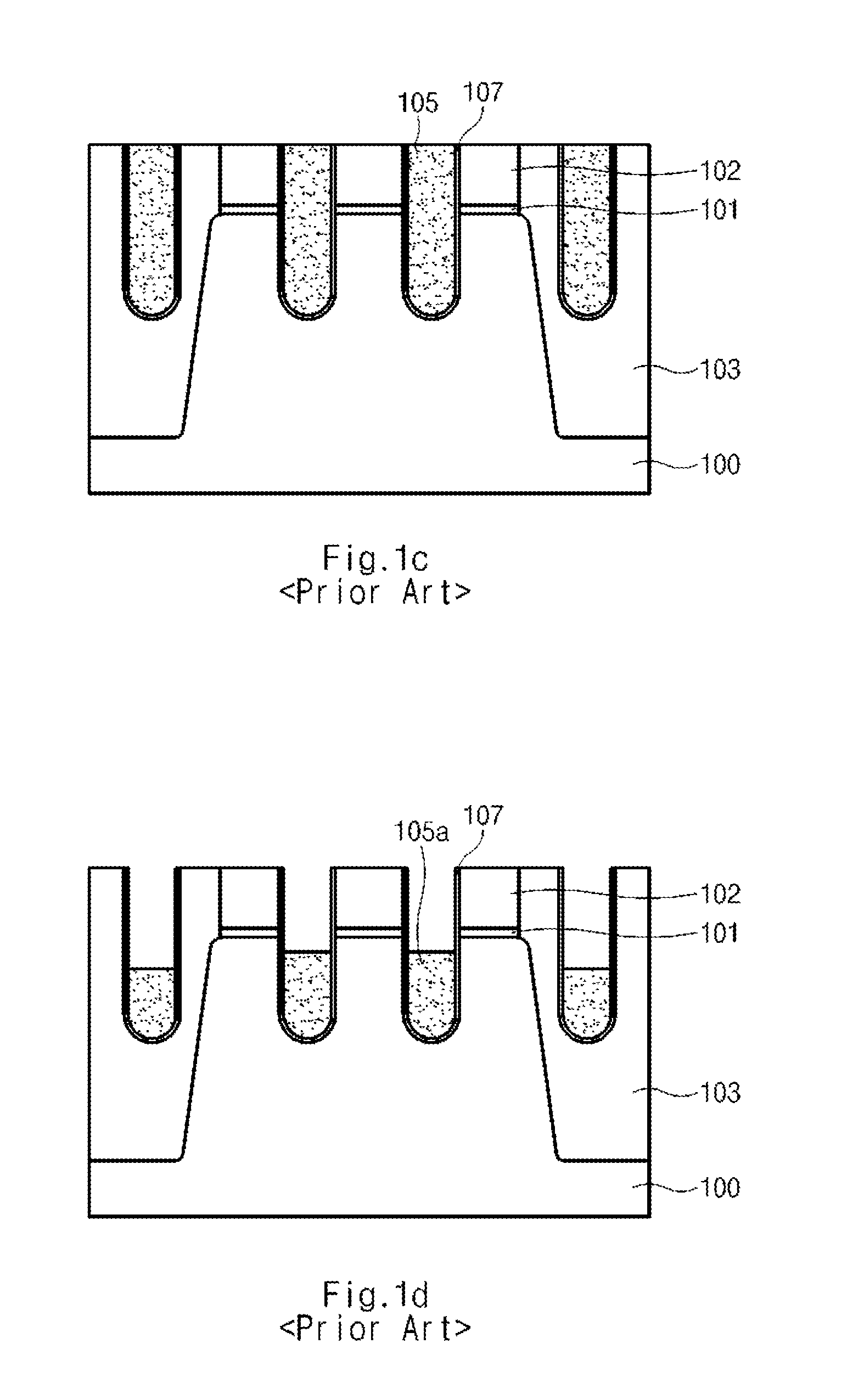
As illustrated in FIG. 2, as an electric field applied to a gate oxide layer increases in a region where the gate is overlapped with a storage node contact region formed on a lateral side of a buried gate, the occurrence of GIDL increases in the corresponding region, resulting in degradation in the refresh characteristic of the semiconductor memory device.
Under those circumstances, further increase of the channel dose by excessive etching of the metal layer may cause an increase of GIDL occurrence and degrade the refresh characteristic of the semiconductor memory device.

Method used


Image

  • Semiconductor memory device and method for fabricating the same
  • Semiconductor memory device and method for fabricating the same
  • Semiconductor memory device and method for fabricating the same

Examples


Embodiment Construction

[0043]A detailed description of the present invention will now be made with reference to the accompanying drawings. Wherever possible, the same reference numbers will be used throughout the drawings to refer to the same or like elements.

[0044]FIGS. 3a to 3e are cross-sectional views illustrating a method for fabricating a semiconductor memory device with a buried gate structure according to an embodiment of the present invention.

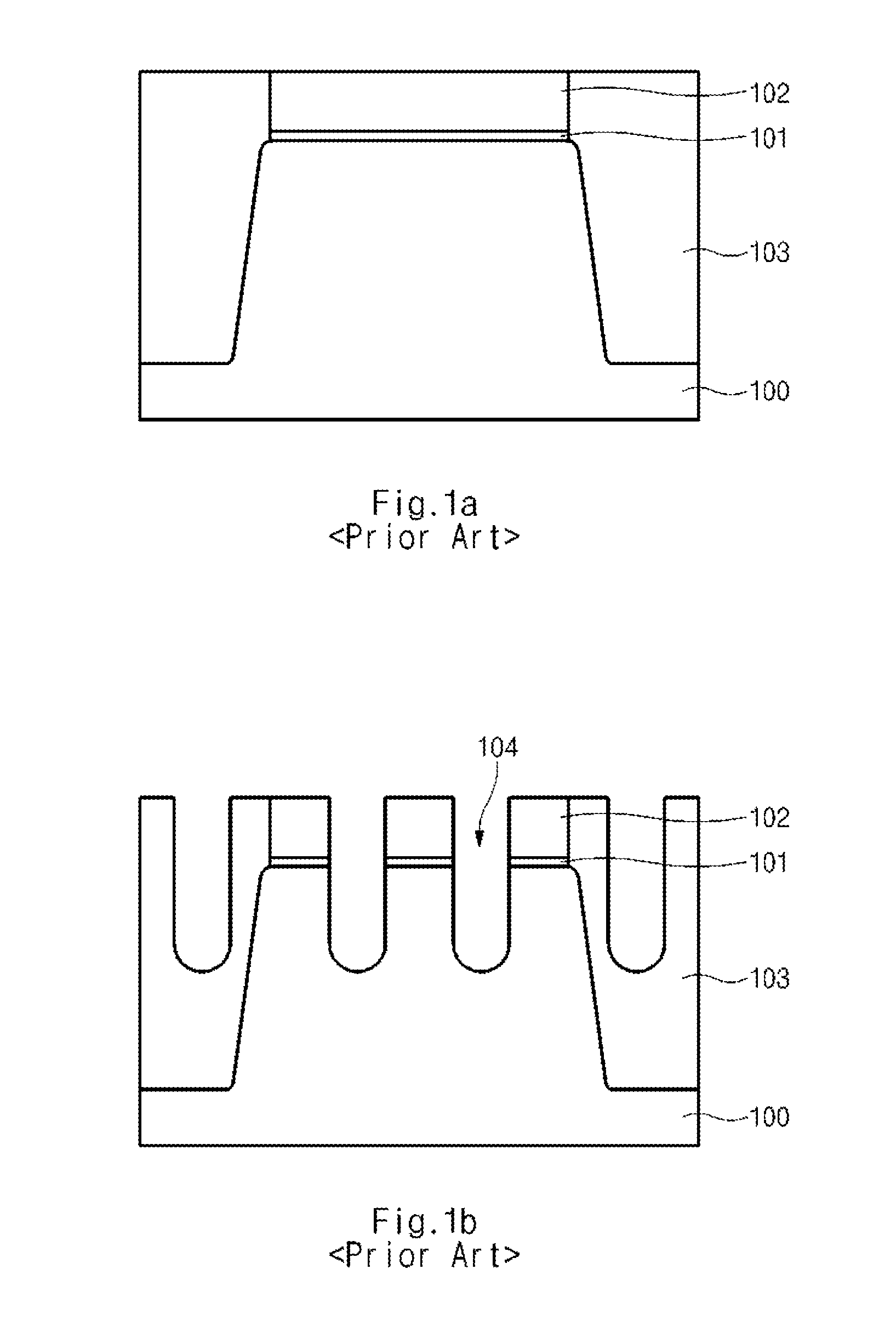
[0045]Referring to FIG. 3a, a pad oxide layer 301 and a pad nitride layer 302 as insulating layers are sequentially deposited on a semiconductor substrate 300. Using an STI process, an isolation layer 303 is formed to define an active region within the semiconductor substrate 300.

[0046]Referring to FIG. 3b, an etch process using a recess gate mask is performed on the active region and the isolation layer 303 to form recesses 304 within the active region and the isolation layer 303. Two recesses 304 are formed in the active region, and one recess 304 is forme...


PUM


Abstract

A semiconductor memory device has an asymmetric buried gate structure with a stepped top surface and a method for fabricating the same. The method for fabricating the semiconductor memory device includes: etching a predetermined region of a semiconductor substrate to form an isolation layer defining an active region; forming a recess within the active region; forming a metal layer filling the recess; asymmetrically etching the metal layer to form an asymmetric gate having a stepped top surface at a predetermined portion of the recess; and forming a capping oxide layer filling a remaining portion of the recess where the asymmetric gate is not formed, thereby obtaining an asymmetric buried gate including the asymmetric gate and the capping oxide layer.

Description

CROSS-REFERENCE TO RELATED APPLICATION[0001]Priority to Korean patent application number 10-2009-0058727, filed on Jun. 30, 2009, which is incorporated by reference in its entirety, is claimed.BACKGROUND OF THE INVENTION[0002]The present invention relates to a method for fabricating a highly-integrated semiconductor memory device, and more specifically, to a semiconductor memory device with a buried gate structure with improved operation characteristics, and a method for fabricating the same.[0003]A common semiconductor memory device includes a plurality of unit cells each of which has a capacitor and a transistor. The capacitor temporarily stores data, and the transistor transfers data between a bit line and a capacitor in response to a control signal (which is applied to a word line) by using a semiconductor property that electrical conductivity varies according to environments. The transistor has three regions: a gate, a source, and a drain. Electric charges move between the sour...

Claims


Application Information

Patent Timeline
Patent Type & Authority Applications(United States)
IPC IPC(8): H01L27/06H01L21/77H10B12/00
CPCH01L21/823437H01L27/0629H01L27/10855H01L29/66621H01L27/10888H01L29/4236H01L29/42376H01L27/10876H10B12/0335H10B12/053H10B12/485H01L21/108
Inventor YANG, HEE JUNG
Owner SK HYNIX INC
Learn More