Method of operating nonvolatile memory device and nonvolatile memory device for implementing the same

a nonvolatile memory and nonvolatile technology, applied in the field of nonvolatile memory devices, can solve the problems of increased production cost, increased area, and increased error rate of cells coupled to the even bit line, and achieve the effect of improving the performance of ecc processing more efficiently

Inactive Publication Date: 2010-12-30
SK HYNIX INC
View PDF5 Cites 12 Cited by
  • Summary
  • Abstract
  • Description
  • Claims
  • Application Information

AI Technical Summary

Benefits of technology

[0010]Exemplary embodiments relate to a nonvolatile memory device and a method of reading the same,

Problems solved by technology

However, the error rate of the cells coupled to the even bit line is not equal to the error rate of the cells coupled to the odd bit line.
In the case in which when the error rate of the cells c

Method used


Image

  • Method of operating nonvolatile memory device and nonvolatile memory device for implementing the same
  • Method of operating nonvolatile memory device and nonvolatile memory device for implementing the same
  • Method of operating nonvolatile memory device and nonvolatile memory device for implementing the same

Examples


Embodiment Construction

[0030]Hereinafter, exemplary embodiments of this disclosure will be described in detail with reference to the accompanying drawings. The figures and description are provided to enable those having ordinary skill in the art to practice the invention without undue experimentation.

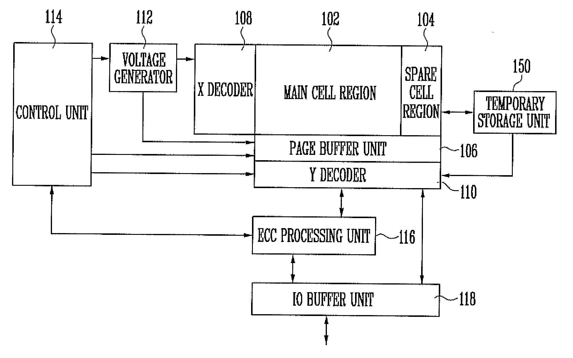
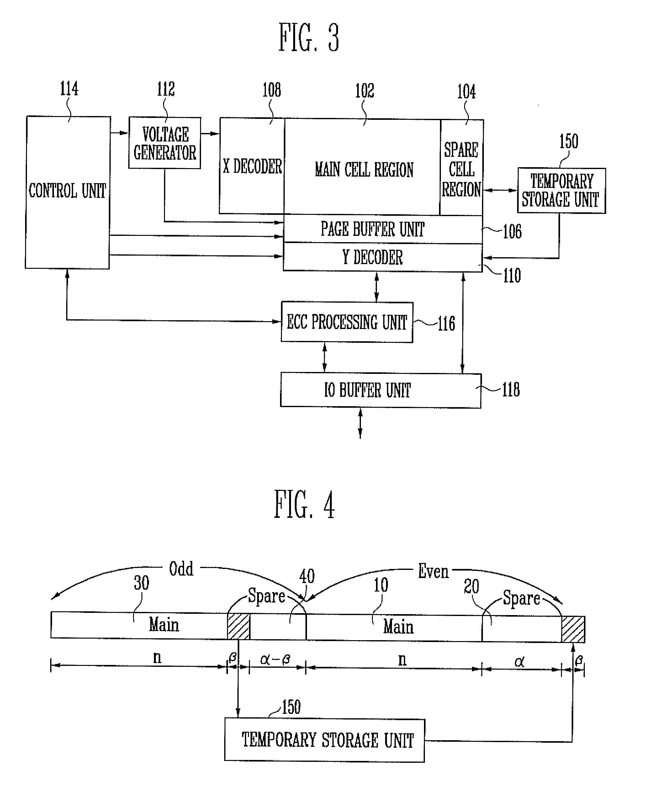
[0031]FIG. 3 is a block diagram showing the internal construction of a nonvolatile memory device according to an embodiment of this disclosure.

[0032]The nonvolatile memory device includes a main cell region 102, a spare cell region 104, a page buffer unit 106, an X decoder 108, a Y decoder 110, a voltage generator 112, a control unit 114, an ECC processing unit 116, an IO buffer unit 118, and a temporary storage unit 150.

[0033]The control unit 114 performs a general control operation of the nonvolatile memory device and generates a program command, an erase command, or a read command in response to a signal transmitted or received through the IO buffer unit 118.

[0034]The voltage generator 112 generates bias v...


PUM


Abstract

A method of operating a nonvolatile memory device including a memory cell array having first and second main cells for storing external input data, first spare cells for storing data for error correction code (ECC) processing on the data stored in the first and second main cells and second spare cells for storing data for ECC processing on the data stored in the first and second main cells which involves reading the data stored in the first spare cells, reading the data stored in the second main cells and the data stored in the second spare cells, and performing the ECC processing on the data read from the second main cells using the data read from the first spare cells and the data read from the second spare cells.

Description

CROSS-REFERENCE TO RELATED APPLICATION[0001]Priority to Korean patent application number 10-20090059147 filed on Jun. 30, 2009, the entire disclosure of which is incorporated by reference herein, is claimed.BACKGROUND[0002]Exemplary embodiments relate to a nonvolatile memory device and, more particularly, to a read method capable of correcting error using spare cells in a nonvolatile memory device.[0003]Recently, there is an increasing demand for nonvolatile memory devices which can be electrically programmed and erased and which do not require the refresh function of rewriting data at specific intervals.[0004]FIG. 1 is a diagram showing the construction of the memory cell array of a known nonvolatile memory device. The memory cell array includes a number of memory cell blocks, but only one memory cell block is illustrated, for the sake of simplified description.[0005]The memory cell array includes a number of memory cell blocks. Each of the memory cell blocks includes a number of s...

Claims


Application Information

Patent Timeline
IPC IPC(8): H03M13/05G06F11/10
CPCG06F11/1008G11C16/0483G11C16/10H03M13/27G11C2029/0411H03M13/13G11C16/26G11C16/34G11C29/42
Inventor LEE, SANG KYUCHUNG, SEUNG JAE
Owner SK HYNIX INC
Why Eureka
Try Eureka