Nanoscale wire-based memory devices

a memory device and nanoscale technology, applied in semiconductor devices, digital storage, instruments, etc., can solve the problem that the field of nanoelectronics is not well-developed

Inactive Publication Date: 2011-01-06
PRESIDENT & FELLOWS OF HARVARD COLLEGE
View PDF6 Cites 14 Cited by
  • Summary
  • Abstract
  • Description
  • Claims
  • Application Information

AI Technical Summary

Benefits of technology

[0014]In another aspect, the present invention is directed to a method of making one or more of the embodiments described herein, for example, a memory device comprising a nanoscale wire. In another aspect, the present invention is directed to a method of using one or more of the embodiments described herein, for example, a memory device comprising a nanoscale wire.
[0015]Other advantages and novel features of the present invention will become apparent from the following detailed description of various non-limiting embodiments of the invention when considered in conjunction with the accompanying figures. In cases where the present specification and a document incorporated by reference include conflicting and / or inconsistent disclosure, the present specification shall control. If two or more documents incorporated by reference include conflicting and / or inconsistent disclosure with respect to each other, then the document having the later effective date shall control.

Problems solved by technology

While nanoscopic articles might be well-suited for transport of charge carriers and excitons (e.g. electrons, electron pairs, etc.) and thus may be useful as building blocks in nanoscale electronics applications, other than standard small-scale lithographic techniques, nanoelectronics is not a well-developed field.

Method used


Image

  • Nanoscale wire-based memory devices
  • Nanoscale wire-based memory devices
  • Nanoscale wire-based memory devices

Examples


example 1

[0081]This example illustrates cross point hysteretic resistance switches based on a core-shell nanowire-metal nanowire crossbar in which the core / shell nanowire core acts as one electrode contact, the shell, which can be controlled synthetically, functions as the storage medium, and the metal nanowire serves as the second electrode contact.

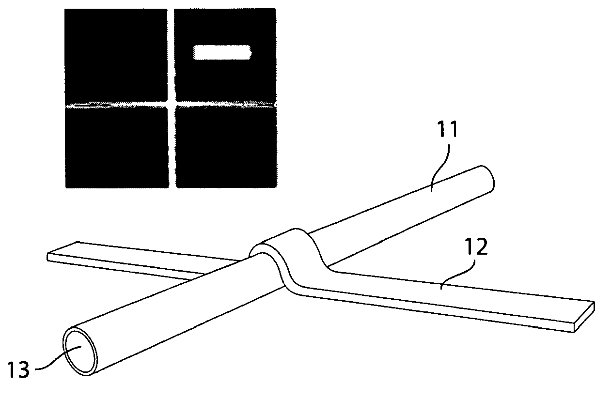
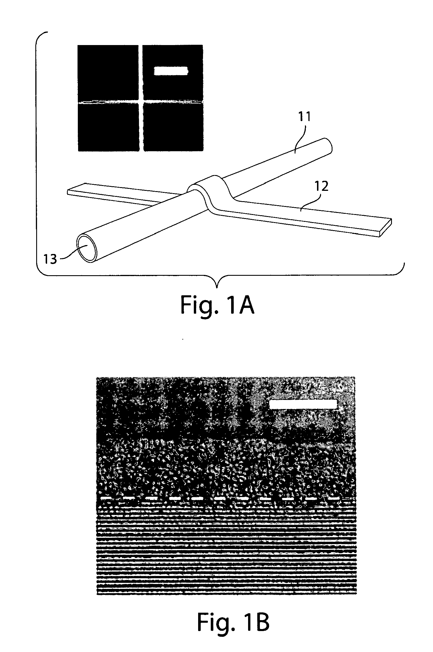
[0082]FIG. 1A shows a Si / a-Si core / shell nanowire (crystalline silicon / amorphous silicon) and a lithographically defined crossed metal nanowire. A single switch is formed at the cross point of a Si (11) / a-Si (13) core / shell nanowire and a metal nanowire (12). The inset is an SEM image of a Si / a-Si nanowire (horizontal) crossed Ag-metal nanowire (vertical) device; the scale bar is 1 micrometer. The core-shell nanowires used in this structure were synthesized in a two step chemical vapor deposition process developed previously, which involves (i) metal nanocluster-catalyzed Si nanowire core growth followed by (ii) homogeneous deposition of the amor...

example 2

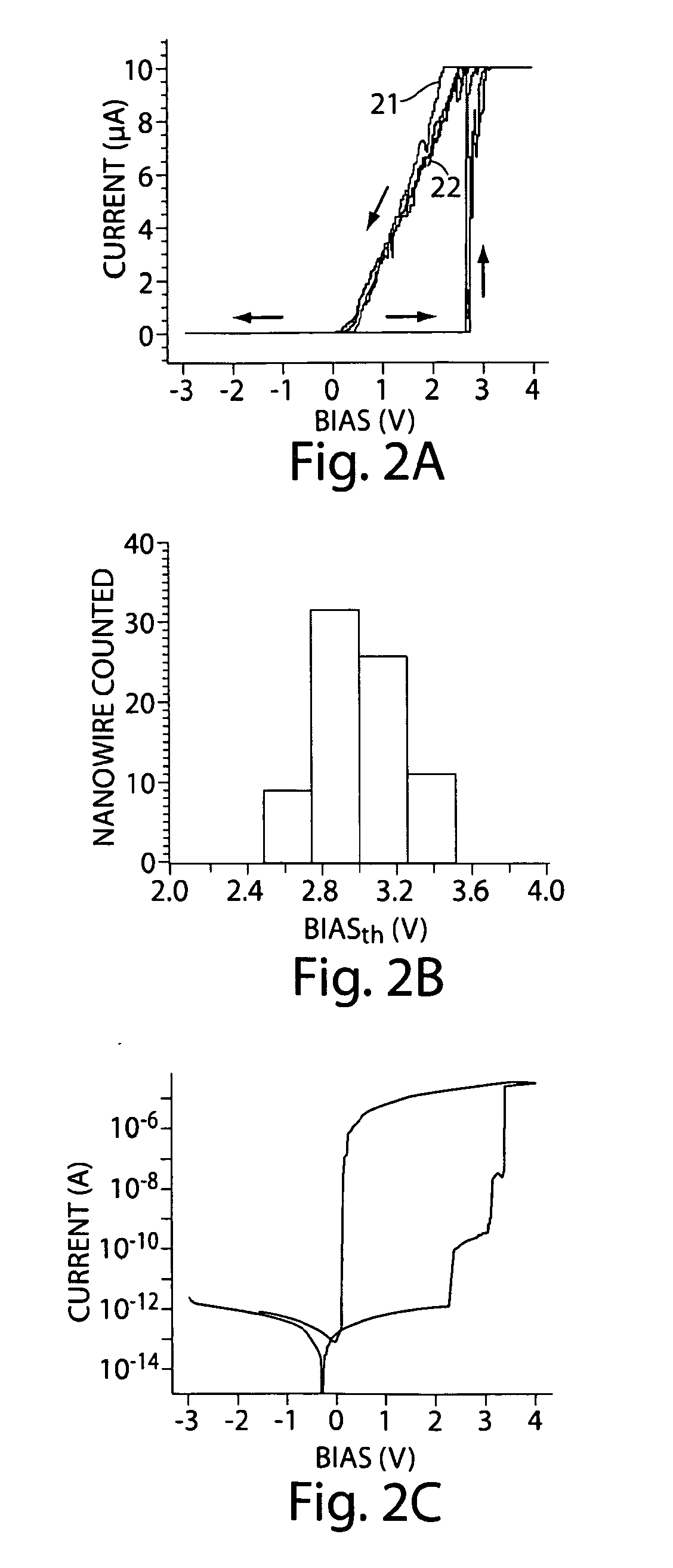
[0101]This example illustrates an example circuit useful for tuning the current applied to the device. In some cases, by tuning this programming circuit, multiple on-resistance states can be found in a single cross point, as is demonstrated in FIGS. 10-11 In FIG. 10, voltage is supplied using DAC (a digital-analog converter) to a nanowire device of the invention, e.g., one containing a Si / a-Si×Ag nanowire. In electrical communication with the Si / a-Si×Ag nanowire is a serial resistor, and a preamplifier unit, before ending with an ADC (an analog-digital converter). FIG. 11 shows that, by controlling the resistance, the current needed to reach the “ON” state can be controlled. However, it should be understood that these components are by way of example only, and in other embodiments, other methods may be used to control the current needed to reach the “ON” state.

[0102]While several embodiments of the present invention have been described and illustrated herein, those of ordinary skill...


PUM


Abstract

The present invention generally relates to nanotechnology and sub-microelectronic devices that can be used in circuitry, and, in particular, to nanoscale wires and other nanostructures able to encode data. One aspect of the present invention is directed to a device comprising an electrical crossbar array comprising at least two crossed wires at a cross point. In some cases, at least one of the crossed wires is a nanoscale wire, and in certain instances, at least one of the crossed wires is a nanoscale wire comprising a core and at least one shell surrounding the core. For instance, the core may comprise a crystal (e.g., crystalline silicon) and the shell may be at least partially amorphous (e.g., amorphous silicon). In certain embodiments, the cross point may exhibit intrinsic current rectification, or other electrical behaviors, and the cross point can be used as a memory device. For example, in one embodiment, the cross point may exhibit a first conductance at a positive voltage, and the cross point may exhibit a second conductance at a negative voltage. Accordingly, by applying suitable voltages to the cross point, data may be stored at the cross point. Other aspects of the present invention are directed to systems and methods for making or using such devices, kits involving such devices, or the like.

Description

RELATED APPLICATIONS[0001]This application claims the benefit of U.S. Provisional Patent Application Ser. No. 61 / 022,497, filed Jan. 21, 2008, entitled “Si / a-Si Core / Shell Nanowires as Nonvolatile Crossbar Switches,” by Lieber, et al.; and U.S. Provisional Patent Application Ser. No. 61 / 011,919, filed Jan. 22, 2008, entitled “Nanoscale Wire-Based Memory Devices,” by Lieber, et al., each incorporated herein by reference.GOVERNMENT FUNDING[0002]Research leading to various aspects of the present invention were sponsored, at least in part, by DARPA. The U.S. Government has certain rights in the invention.FIELD OF INVENTION[0003]The present invention generally relates to nanotechnology and sub-microelectronic devices that can be used in circuitry and, in particular, to nanoscale wires and other nanostructures able to encode data.BACKGROUND[0004]Interest in nanotechnology, in particular sub-microelectronic technologies such as semiconductor quantum dots and nanowires, has been motivated b...

Claims


Application Information

Patent Timeline
Patent Type & Authority Applications(United States)
IPC IPC(8): H01L29/66H01L21/60
CPCB82Y10/00G11C13/0002H01L2924/0002G11C13/0069G11C2213/77G11C2213/81H01L27/10H01L27/101H01L29/0665H01L29/0673H01L29/16H01L29/1602H01L29/1604H01L2924/00
Inventor LIEBER, CHARLES M.DONG, YAJIELU, WEIYU, GUIHUAMEALPHINE, MICHAEL
Owner PRESIDENT & FELLOWS OF HARVARD COLLEGE
Why Eureka
Try Eureka