Semiconductor light-emitting device with double-sided passivation

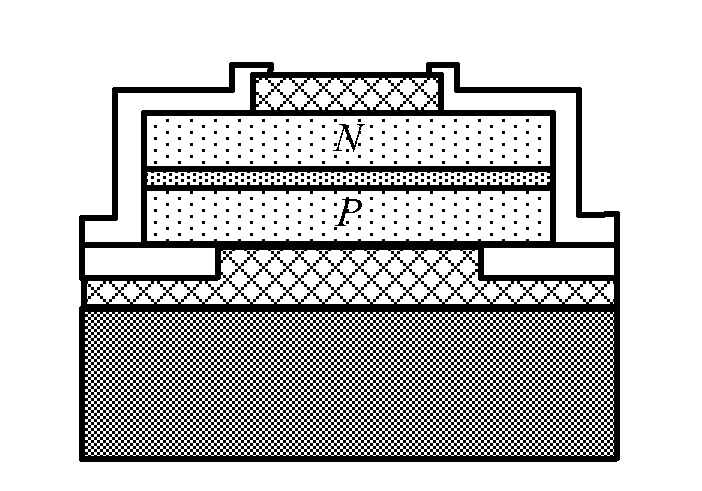
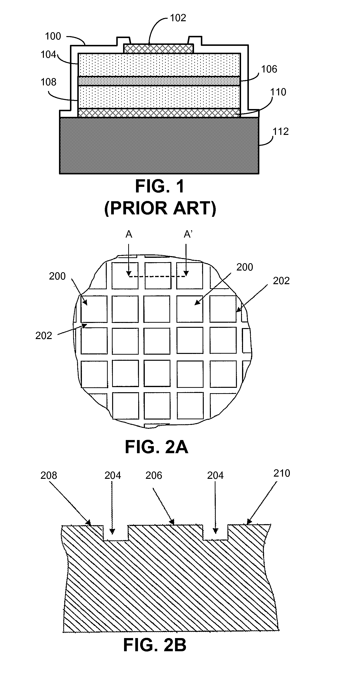
a semiconductor and light-emitting device technology, applied in the field of design of semiconductor light-emitting devices, can solve the problems of increasing impurities and defects, severely degrading the reliability and stability of leds, and sidewall coverage of a conventional passivation layer, for example, the layer b>100/b> shown in fig. 1, is often non-ideal, and achieves the effect of reducing surface recombination

Active Publication Date: 2011-01-06
LATTICE POWER (JIANGXI) CORP
View PDF11 Cites 11 Cited by
  • Summary
  • Abstract
  • Description
  • Claims
  • Application Information

AI Technical Summary

Benefits of technology

[0010]One embodiment of the present invention provides a light-emitting device. The device includes a substrate, a first doped semiconductor layer situated above the substrate, a second doped semiconductor layer situated above the first doped semiconductor layer, and a multi-quantum-well (MQW) active layer situated between the first and the second doped semiconductor layers. The device also includes a first electrode coupled to the first doped semiconductor layer and a first passivation layer, which is situated between the first electrode and the first doped semiconductor layer in areas other than an ohmic-contact area. The first passivation layer substantially insulates the first electrode from edges of the first doped semiconductor layer, thereby reducing surface recombination. The device further includes a second electrode coupled to the second doped semiconductor layer and a second passivation layer which substantially covers the sidewalls of the first and second doped semiconductor layer, the MQW active layer, and part of the horizontal surface of the second doped semiconductor layer which is not covered by the second electrode.

Problems solved by technology

However, due to the abrupt termination of the crystal structure at the lateral surface of the LED, there are large numbers of recombination centers on such surface.
In addition, the surface of an LED is very sensitive to its surrounding environment, which may lead to added impurities and defects.
Environmentally induced damage can severely degrade the reliability and stability of an LED.
However, the sidewall coverage by a conventional passivation layer, for example, layer 100 shown in FIG. 1, is often non-ideal.
The poor sidewall coverage is typically a result of standard thin-film deposition techniques, such as plasma-enhanced chemical vapor deposition (PECVD) and magnetron sputtering deposition.
The quality of sidewall coverage by passivation layer is worsened for devices with steeper steps, such as devices with steps higher than 2 μm, which is the case for most vertical-electrode LEDs.
Under such conditions, the passivation layer often contains a large number of pores, which can severely degrade its ability to block the surface recombination of carriers.
An increased surface recombination rate in turn increases the amount of the reverse leakage current, which results in reduced efficiency and stability of the LED.

Method used


Image

  • Semiconductor light-emitting device with double-sided passivation
  • Semiconductor light-emitting device with double-sided passivation
  • Semiconductor light-emitting device with double-sided passivation

Examples


examples

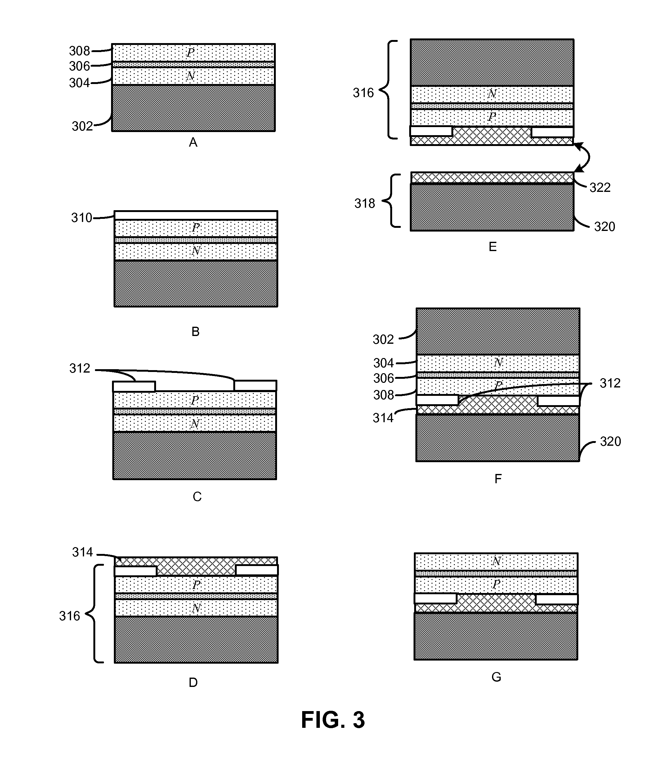
[0039]In one embodiment, a conventional substrate is patterned and etched to form individual mesas. Each mesa has a size of approximately 300×300 μm2. A 500-angstrom-thick SiO2 layer forms the bottom passivation layer, and a 2,000-angstrom-thick SiO2 layer forms the top passivation layer. After etching, the size of the p-side electrode is approximately 250×250 μm2. The top surface area of the device after edge removal is approximately 280×280 μm2.

[0040]In one embodiment, each mesa has a size of approximately 300×300 μm2. A 500-angstrom-thick SiO2 layer forms the bottom passivation layer, and a 2,000-angstrom-thick SiNx layer forms the top passivation layer. After etching, the size of the p-side electrode is approximately 250×250 μm2. The top surface area of the device after edge removal is approximately 280×280 μm2.

[0041]In one embodiment, each mesa has a size of approximately 300×300 μm2. A 100-angstrom-thick SiNx layer forms the bottom passivation layer, and a 5,000-angstrom-thick...


PUM


Abstract

A light-emitting device includes a substrate, a first doped semiconductor layer situated above the substrate, a second doped semiconductor layer situated above the first doped layer, and a multi-quantum-well (MQW) active layer situated between the first and the second doped layers. The device also includes a first electrode coupled to the first doped layer and a first passivation layer situated between the first electrode and the first doped layer in areas other than an ohmic-contact area. The first passivation layer substantially insulates the first electrode from edges of the first doped layer, thereby reducing surface recombination. The device further includes a second electrode coupled to the second doped layer and a second passivation layer which substantially covers the sidewalls of the first and second doped layers, the MQW active layer, and the horizontal surface of the second doped layer.

Description

[0001]This application is a U.S. National Stage application under 35 U.S.C. section 371 of PCT Application No. PCT / CN2008 / 000581, entitled “SEMICONDUCTOR LIGHT-EMITTING DEVICE WITH DOUBLE-SIDED PASSIVATION,” by inventors Fengyi Jiang, Junlin Liu, and Li Wang, filed 25 Mar. 2008.BACKGROUND[0002]1. Field of the Invention[0003]The present invention relates to the design of semiconductor light-emitting devices. More specifically, the present invention relates to novel semiconductor light-emitting devices with double-sided passivation that effectively reduces the leakage current and enhances the device reliability.[0004]2. Related Art[0005]Solid-state lighting is expected to bring the next wave of illumination technology. High-brightness light-emitting diodes (HB-LEDs) are emerging in an increasing number of applications, from serving as the light source for display devices to replacing light bulbs for conventional lighting. Typically, cost, efficiency, and brightness are the three forem...

Claims


Application Information

Patent Timeline
Patent Type & Authority Applications(United States)
IPC IPC(8): H01L33/04H01L21/18H01L33/00H01L33/40H01L33/44
CPCH01L21/6835H01L33/0079H01L2221/68359H01L33/44H01L2221/6835H01L33/405H01L33/0093
Inventor JIANG, FENGYILIU, JUNLINWANG, LI
Owner LATTICE POWER (JIANGXI) CORP
Why Eureka
Try Eureka