Back contact type solar cell based on P-type silicon substrate and manufacturing method thereof

A solar cell and back-contact technology, applied in circuits, photovoltaic power generation, electrical components, etc., can solve the problems of poor surface coverage uniformity of silicon wafers, complex battery process control, and greater influence of P-type silicon wafers. Treatment, reduced surface recombination, easy to pinpoint the effect of doping

Active Publication Date: 2015-12-23
YELLOW RIVER PHOTOVOLTAIC IND TECH CO LTD
View PDF4 Cites 10 Cited by
  • Summary
  • Abstract
  • Description
  • Claims
  • Application Information

AI Technical Summary

Problems solved by technology

This method mainly has the following problems: 1, BBr 3 The reaction produces B 2 o 3 , its boiling point is high, it is still liquid at high temperature, and the surface coverage of the silicon wafer is poor, which is easy to cause the problem of poor diffusion uniformity; 3. Due to the limitations of the current N-type silicon rod drawing technology, its resistivity distribution range (1Ω·cm~12Ω·cm) is much larger than that of P-type silicon wafers (0.5Ω·cm~3Ω cm), the battery process control is more complicated, and the cost of N-type silicon wafers is also an important factor limiting its large-scale application

Method used


Image

  • Back contact type solar cell based on P-type silicon substrate and manufacturing method thereof
  • Back contact type solar cell based on P-type silicon substrate and manufacturing method thereof
  • Back contact type solar cell based on P-type silicon substrate and manufacturing method thereof

Examples


preparation example Construction

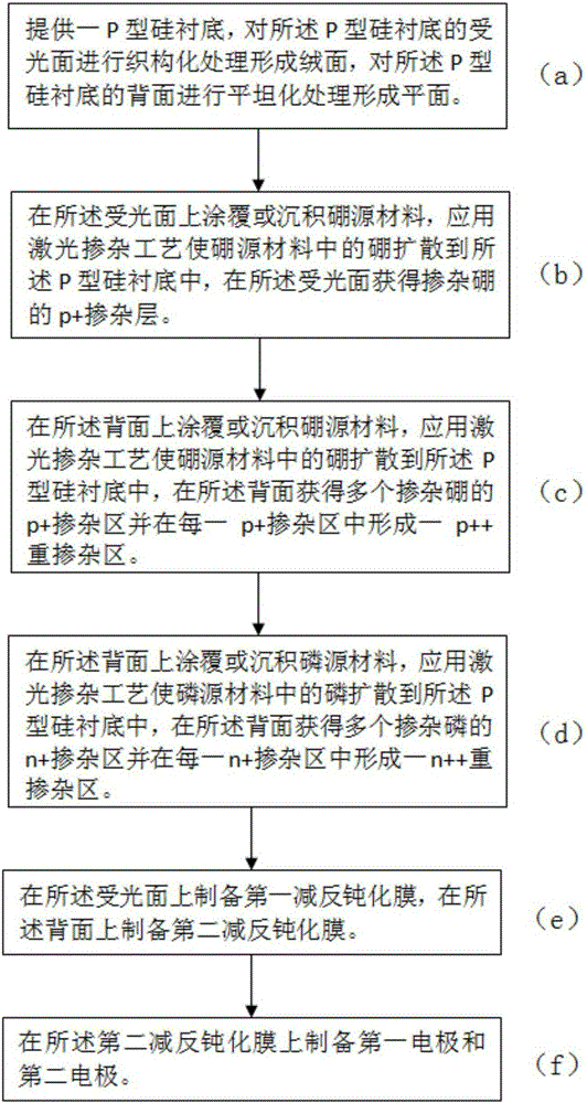
[0033] Introduce the preparation method of above-mentioned solar cell below, as image 3 As shown, the method includes the steps of:

[0034] (a) A P-type silicon substrate is provided, the light-receiving surface of the P-type silicon substrate is textured to form a textured surface, and the back surface of the P-type silicon substrate is planarized to form a plane.

[0035] (b) Coating or depositing a boron source material on the light-receiving surface, applying a laser doping process to diffuse boron in the boron source material into the P-type silicon substrate, and obtaining a boron-doped silicon substrate on the light-receiving surface p+ doped layer. Wherein, the boron source material is selected from boric acid solution, borosilicate glass, boron-containing silicon nitride, boron-containing silicon oxide or boron-containing amorphous silicon.

[0036] (c) Coating or depositing a boron source material on the back surface, applying a laser doping process to diffuse bo...

Embodiment 1

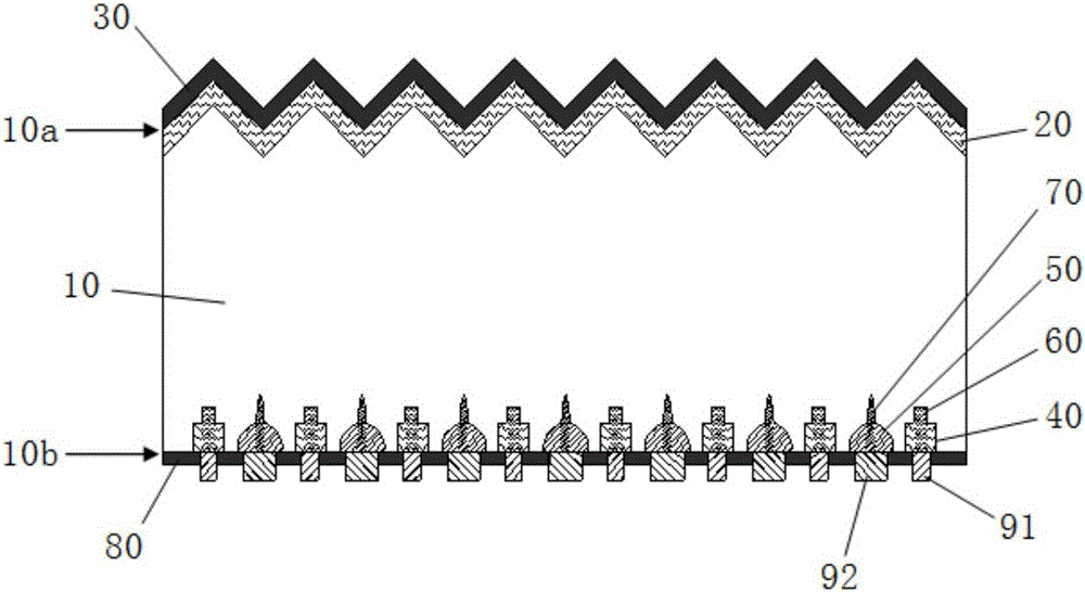
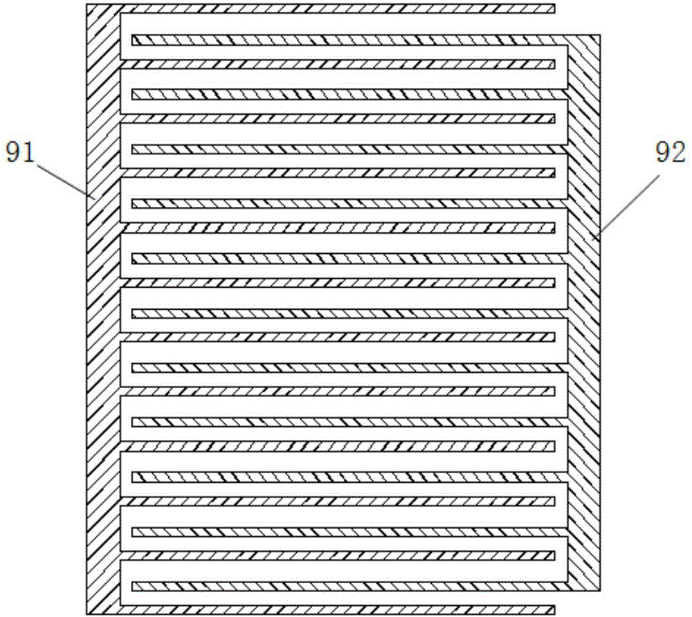
[0046] 1. If Figure 4a As shown, firstly, a P-type silicon substrate 10 is provided, which includes a light-receiving surface 10a and a back surface 10b opposite to each other. Surface texturing treatment is carried out on the light-receiving surface 10a of the P-type silicon substrate 10: specifically, a mixed solution of potassium hydroxide or sodium hydroxide, IPA and texturing additives can be used for surface treatment, and the surface is pyramid-shaped. surface structure; after the texturing treatment, the silicon substrate 10 is chemically cleaned. Perform planarization treatment on the back surface 10b of the P-type silicon substrate 10: specifically, first use SiO on the light-receiving surface 10a 2 、SiN x etc. to protect the dielectric film, and then directly etch the backside in potassium hydroxide or sodium hydroxide alkali solution (10% mass fraction), or use HF / HNO 3 The mixed acid solution is used for back etching, and after the etching is completed, the si...

Embodiment 2

[0053] The difference between this embodiment and Embodiment 1 is that in this embodiment, the order of Step 2 and Step 3 in Embodiment 1 is reversed, that is, after the P-type silicon substrate 10 is processed, an n+ doped substrate is first prepared on the back surface 10b. For the impurity region 50 and the n++ heavily doped region 70, refer to step 3 in Embodiment 1; Step 2 in Example 1. The rest of the steps are the same as those in Embodiment 1 and will not be repeated here.

[0054] Compared with the prior art, the present invention uses a P-type silicon chip as the substrate material, which is low in cost and widely used. Back planarization treatment, that is, back polishing, is conducive to the formation of uniform PN junctions and PP+ high-low junctions on the back, while reducing the specific surface area of ​​the back and reducing surface recombination. The doping source adopts liquid or solid state, which is safe and reliable, and is also conducive to laser trea...


PUM


Abstract

The invention discloses a back contact type solar cell based on a P-type silicon substrate. One P-type silicon substrate is included. An illuminated surface of the P-type silicon substrate is provided with a p+ doping layer doped with boron. The illuminated surface is provided with a first anti-reflection passive film. A back side of the P-type silicon substrate is provided with a plurality of p+ doping regions doped with boron and a plurality of n+ doping regions doped with phosphori. Each p+ doping region is provided with one p++ heavily doped region. Each n+ doping region is provided with one n++ heavily doped region. A back side is provided with a second anti-reflection passive film. The second anti-reflection passive film is provided with a first electrode and a second electrode which are mutually insulated. The first electrode and the second electrode are electrically connected to the p++ heavily doped region and the n++ heavily doped region. The invention also discloses a manufacturing method of the solar cell. A P-type silicon wafer is used as a substrate material of the back contact type solar cell. A technology of the P-type silicon wafer is mature and an obvious cost advantage is possessed.

Description

technical field [0001] The invention relates to the field of solar cell manufacturing with a new structure, in particular to a back-contact solar cell based on a P-type silicon substrate and a preparation method thereof. Background technique [0002] With the shortage of global energy and climate warming, renewable energy such as solar power is replacing traditional thermal power, and has become a research hotspot and development trend in the energy field today. In the development history of solar cells, both amorphous silicon thin film solar cells and crystalline silicon solar cells have experienced more than half a century of development. Crystalline silicon solar cells are more efficient, while amorphous silicon thin-film solar cells are less expensive to manufacture. In traditional P-type silicon substrate solar cells, the PN junction is formed by high-temperature diffusion. The PN junction is on the front side and the electrodes are on both sides of the solar cell. The...

Claims


Application Information

Patent Timeline
Patent Type & Authority Applications(China)
IPC IPC(8): H01L31/068H01L31/0224H01L31/18
CPCH01L31/022425H01L31/0682H01L31/1804H01L31/0224H01L31/068H01L31/18Y02E10/547Y02P70/50
Inventor 郭灵山崇锋吕欣
Owner YELLOW RIVER PHOTOVOLTAIC IND TECH CO LTD
Why Eureka
Try Eureka