Method for manufacturing semicondutor device with strained channel

a technology of strained channel and semiconductor device, which is applied in the direction of semiconductor devices, basic electric elements, electrical equipment, etc., can solve the problems of increasing gate leakage current, short channel effect, and reducing the thickness of gate insulating layer, so as to maximize the strained channel effect and suppress the short channel effect

Inactive Publication Date: 2011-01-06
SK HYNIX INC
View PDF22 Cites 210 Cited by
  • Summary
  • Abstract
  • Description
  • Claims
  • Application Information

AI Technical Summary

Benefits of technology

Embodiments of the present invention are directed to providing a method for manufacturing a semicon

Problems solved by technology

However, the reduction of a channel length disadvantageously causes short channel effect.
Further, the reduction of the gate insulating layer thickness increases gate leakage current.
That is, the doped impurities disturb carrier movement.
However, when a channel length becomes short due to the high integration of a device, or when a deep recess is formed and In-Situ doping is performed, a junction depth becomes significantly large.
In other words, although a recess depth should be deep for obtaining a strained channel effect, the short channel eff

Method used


Image

  • Method for manufacturing semicondutor device with strained channel
  • Method for manufacturing semicondutor device with strained channel
  • Method for manufacturing semicondutor device with strained channel

Examples


Embodiment Construction

Other objects and advantages of the present invention can be understood by the following description, and become apparent with reference to the embodiments of the present invention.

FIGS. 2A to 2E are diagrams illustrating a method for fabricating a semiconductor device having a strained channel in accordance with an embodiment of the present invention.

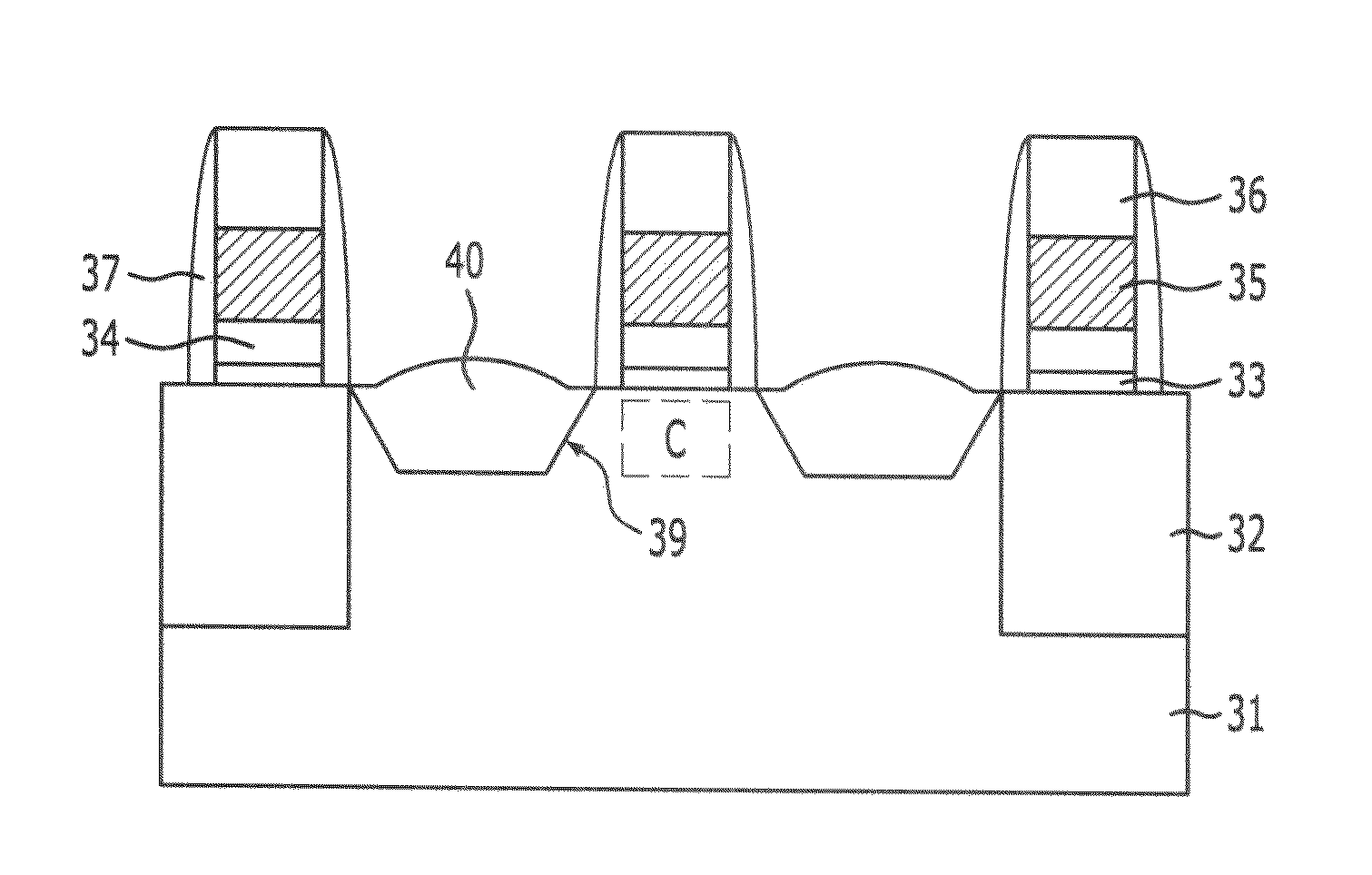
As shown in FIG. 2A, a field oxide layer 32 is formed in a silicon substrate 31 to isolate one device from another. The field oxide layer 32 may be formed using an STI process. The field oxide layer 32 defines an active area.

A gate pattern including a gate insulating layer 33, a gate polysilicon layer 34, a gate conductive layer 35, and a gate hard mask layer 36 is formed. A channel region C is formed below the gate pattern.

Gate spacers 37 are formed on both sidewalls of the gate pattern. The gate spacers 37 may be formed by depositing a spacer insulating layer and etching back the spacer insulating layer.

The spacer insulating layer us...


PUM


Abstract

A method for forming a semiconductor device includes forming a gate pattern over a silicon substrate, forming gate spacers over both sidewalls of the gate pattern, forming a dummy gate spacer over a sidewall of each one of the gate spacers, forming a recess region having inclined sidewalls extending in a direction to a channel region under the gate pattern by recess-etching the silicon substrate, filling the recess region with an epitaxial film, which becomes a source region or a drain region, through a selective epitaxial growth process, and removing the dummy gate spacer.

Description

CROSS-REFERENCE TO RELATED APPLICATIONSThe present application claims priority of Korean patent application number 10-2009-0060876, filed on Jul. 3, 2009, which is incorporated by reference in its entirety.BACKGROUND OF THE INVENTIONThe present invention relates to a method for fabricating a semiconductor device, and more particularly, to a method for fabricating a semiconductor device having a strained channel.Due to the high-integration of a semiconductor device, a gate insulating layer thickness and a channel length of a MOS device have been continuously reduced. Such reduction of the gate insulating layer thickness and the channel length increases the mobility of electrons or holes. That is, the reduction of the gate insulating layer thickness and the channel length improves the speed and operation current of a device.However, the reduction of a channel length disadvantageously causes short channel effect. Further, the reduction of the gate insulating layer thickness increases g...

Claims


Application Information

Patent Timeline
IPC IPC(8): H01L21/336
CPCH01L29/165H01L29/6653H01L29/7848H01L29/78H01L29/66636H01L29/66348
Inventor LEE, YOUNG-HOAHN, TAE-HANGBAEK, SEUNG-BEOMCHO, JUN-HEEKIM, JEONG-SEON
Owner SK HYNIX INC
Why Eureka
Try Eureka