Method for manufacturing electronic component module

a technology of electronic components and manufacturing methods, applied in the direction of resistive material coating, solid-state device coating, metallic material coating process, etc., can solve the problems of voids within the resin layer, electronic components may not be adequately shielded from electric field noise and electromagnetic wave noise, and the bottom of the groove section may be incompletely filled or filled, etc., to achieve a lower profile and lower profile

Active Publication Date: 2011-01-13
MURATA MFG CO LTD
View PDF7 Cites 22 Cited by
  • Summary
  • Abstract
  • Description
  • Claims
  • Application Information

AI Technical Summary

Benefits of technology

[0015]The collective substrate including the plurality of electronic component modules defined by the plurality of electronic components is preferably batch-sealed with a resin, and the cut section is formed from the top surface of the sealed resin to the position that reaches the grounding electrode arranged in the substrate, at the boundary section of the electronic component module. After applying the conductive paste on the side surfaces and the top surface, the conductive paste formed on the side surfaces and top surface of the electronic component module can be made into a thin film (for example, about 5 μm to about 15 μm) by spin coating, so as to produce an electronic component module having a lower profile. Furthermore, since the conductive paste filling the cut section can be also made into a thin film, no voids occur due to vaporization of a diluted solution of the paste in a thermal curing treatment or due to air bubbles remaining in the paste. Therefore, the elimination of a portion having no shield layer formed thereon allows the electronic components to be sufficiently shielded from electric field noises and electromagnetic wave noises. Moreover, similar effects can also be expected in the case of electronic components disposed on an upper surface and a lower surface of the substrate.
[0016]The cross-sectional shape in a direction substantially perpendicular to the cut section at the bottom of the cut section is preferably a curved shape or a shape with a predetermined slope. Thus, a portion with no conductive paste is prevented from occurring when filling the cut section with the conductive paste, thereby preventing the occurrence of voids.
[0017]The grounding electrode of the collective substrate, which is exposed by the formation of the cut section, is preferably provided on each of four side surfaces of the electronic component module, thereby allowing the electronic components to be sufficiently shielded from electric field noises and electromagnetic wave noises. Furthermore, while a difference occurs due to the spin coating in the thickness of the film applied on the cut sections between the direction toward the center of rotation and the direction along the periphery, the grounding electrodes are formed on the four side surfaces, thereby allowing the shielding property for the electronic components, the internal wirings, and other elements of the electronic component module to be improved.
[0018]With the structure described above, after applying the conductive paste on the side surfaces and the top surface of the electronic component module, the conductive paste formed on the side surfaces and top surface of the electronic component module can be made into a thin film (for example, about 5 μm to about 15 μm) by spin coating, so as to produce an electronic component module having a lower profile. Furthermore, since the conductive paste filling the cut section can be also made into a thin film, no voids occur due to vaporization of a diluted solution of the paste in thermal curing or due to air bubbles remaining in the paste, allowing the electronic components to be sufficiently shielded from electric field noises and electromagnetic wave noises.

Problems solved by technology

However, in the manufacturing method disclosed in Japanese Patent Application Laid-Open No. 2004-172176, unless the groove section is to be filled with a relatively large amount of conductive paste with a relatively small viscosity in order to fill the groove section with the conductive paste, the bottom of the groove section may be incompletely filled or filled with the conductive paste including air bubbles.
In this case, as the conductive paste is generally a thermosetting resin, voids will likely occur within the resin layer during curing, leading to a problem in that the electronic components may be insufficiently shielded from electric field noises and electromagnetic wave noises.
However, in this case, the diluted solution may be gasified during curing of the thermosetting resin, which results in voids within the resin layer due to gas from the vaporization of the diluted solution.
Therefore, the use of the diluted solution does not effectively solve the problem that the electronic components may be insufficiently shielded from electric field noises and electromagnetic wave noises.
Therefore, the immersion in the plating solution may cause the plating solution to penetrate into the sealed resin, which may lead to a problem of damage to the electronic components due to the plating solution and decreased reliability due to water absorption by the sealed resin.
Furthermore, in Japanese Patent Application Laid-Open No. 2005-79139, in the case of batch-shielding a plurality of modules, it is difficult to form the shield layer uniformly on side surfaces of the packages unless the groove section between the packages has a sufficiently large width, which leads to a problem that the electronic components may be insufficiently shielded from electric field noises and electromagnetic wave noises.
Furthermore, in the case of spray coating, because a highly flammable conductive resin is sprayed, facilities are required to have explosion-proof specifications, which leads to the problem of high production cost.

Method used


Image

  • Method for manufacturing electronic component module
  • Method for manufacturing electronic component module
  • Method for manufacturing electronic component module

Examples


first preferred embodiment

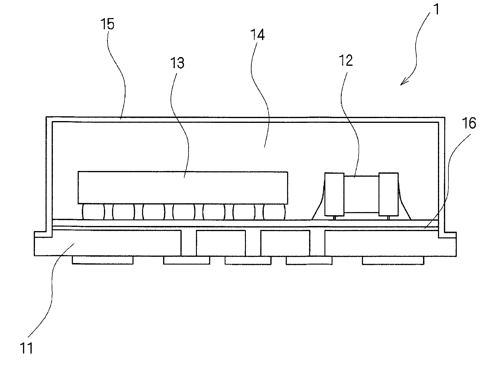
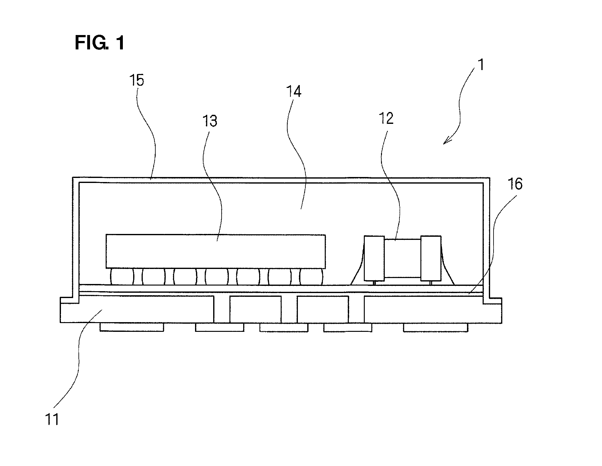
[0032]FIG. 1 is a cross-sectional view illustrating the structure of an electronic component module according to a first preferred embodiment of the present invention. The electronic component module 1 according to the first preferred embodiment of the present invention preferably has, for example, dimensions of about 10.0 mm×about 10.0 mm×about 1.2 mm, and includes a circuit substrate 11 including ceramics, glass, an epoxy resin, or other suitable material, and electronic components 12 and 13, such as semiconductor elements, capacitors, resistors, SAW filters, for example, which are disposed on a surface of the circuit substrate 11.

[0033]The circuit substrate 11 is preferably, for example, a resin substrate having a rectangular upper surface and a thickness of approximately 0.6 mm, for example. The surface of the circuit substrate 11 is provided with a signal pattern (not shown) which also defines a junction pad with the electronic components 12 and 13 and with a grounding electrod...

second preferred embodiment

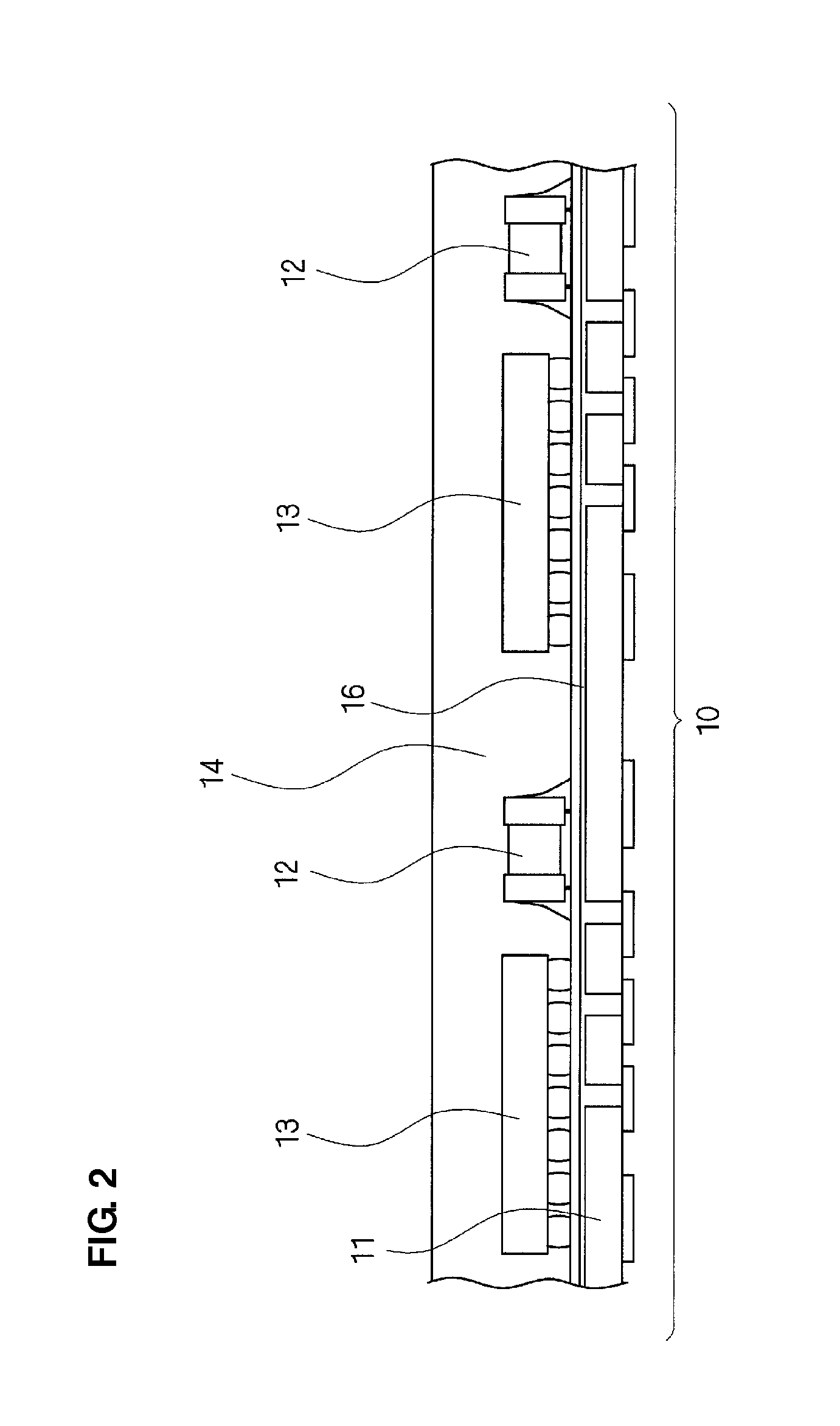
[0047]FIG. 8 is a cross-sectional view illustrating the structure of an electronic component module according to a second preferred embodiment of the present invention. The electronic component module 1 according to the second preferred embodiment of the present invention differs from the first preferred embodiment in that electronic components 12 and 13, such as semiconductor elements, capacitors, resistors, SAW filters, for example, are disposed on both sides of a circuit substrate 11 including ceramics, glass, an epoxy resin, or other suitable material, for example.

[0048]Both sides of the circuit substrate 11 are provided with a signal pattern (not shown) which also defines a junction pad with the electronic components 12 and 13 and with a grounding electrode 16 exposed adjacent to the circuit substrate 11. The signal pattern of the circuit substrate 11 is connected to the terminals of the electronic components 12 and 13, such as each semiconductor element, capacitor, and resisto...

third preferred embodiment

[0055]FIGS. 10A to 10C are cross-sectional views illustrating the structure of an electronic component module 1 according to a third preferred embodiment of the present invention. The electronic component module 1 according to the third preferred embodiment of the present invention differs from the first and second preferred embodiments in that the cross-sectional shape around the conductive connection of a grounding electrode 16 to a shield layer 15 near the bottom of a side section is a curved shape or a shape with a predetermined gradient.

[0056]FIG. 10A is cross-sectional views illustrating the structure of an electronic component module 1 according to the third preferred embodiment of the present invention. A side section shown in FIG. 10A is a view of the cut sections 17 in FIGS. 3 through 5, showing the shape of an edge section A near the bottom. FIG. 10B is a cross-sectional view illustrating a structure of an edge section of an electronic component module 1 according to the ...


PUM

PropertyMeasurementUnit
thicknessaaaaaaaaaa
thicknessaaaaaaaaaa
conductiveaaaaaaaaaa

Abstract

A method for manufacturing an electronic component module is performed such that a shield layer can be formed as a thin film and an electronic component can be effectively shielded. A collective substrate including a plurality of electronic component modules including a plurality of electronic components is batch-sealed with a resin. A cut section is formed from a top surface of the sealed resin to a position that reaches a grounding electrode arranged in the substrate at a boundary section of the electronic component module so as to expose the grounding electrode. A conductive paste is applied on side surfaces and the top surface. Then, a conductive thin film is formed by spin coating, and the electronic component module is cut.

Description

BACKGROUND OF THE INVENTION[0001]1. Field of the Invention[0002]The present invention relates to a method for manufacturing an electronic component module, in which an electronic component module including a grounding electrode extending around the bottom thereof is cut from a collective substrate with a plurality of electronic component modules including a plurality of electronic components.[0003]2. Description of the Related Art[0004]Conventionally, when manufacturing an electronic component module, a collective substrate including a variety of electronic components is batch-sealed with a resin, and a groove (cut) section is formed from a top surface of the sealed resin to a position that reaches a grounding electrode, at a boundary section for cutting into electronic component modules. Then, after filling the groove section with a conductive paste, individual electronic component module units are cut from the boundary section, thereby manufacturing electronic component modules (s...

Claims


Application Information

Patent Timeline
Patent Type & Authority Applications(United States)
IPC IPC(8): B23K31/02
CPCH01L23/552H01L2924/15159H01L25/165H01L25/50H01L2224/97H01L2924/01004H01L2924/01029H01L2924/01033H01L2924/01047H01L2924/01082H01L2924/09701H01L2924/19105H05K1/0218H05K3/0052H05K3/284H05K2201/098H05K2203/1316H01L24/97H01L2924/12041H01L2924/01005H01L2924/01006H01L2924/014H01L2224/16225H01L2224/81H01L2924/3025H01L2924/19106H01L2224/16227
Inventor KANRYO, KOICHIKATSUBE, AKIOTANAKA, AKIRA
Owner MURATA MFG CO LTD
Why Eureka
Try Eureka