Apparatus for driving capacitive light emitting device
- Summary
- Abstract
- Description
- Claims
- Application Information
AI Technical Summary
Benefits of technology
Problems solved by technology
Method used
Image

Examples
example 1
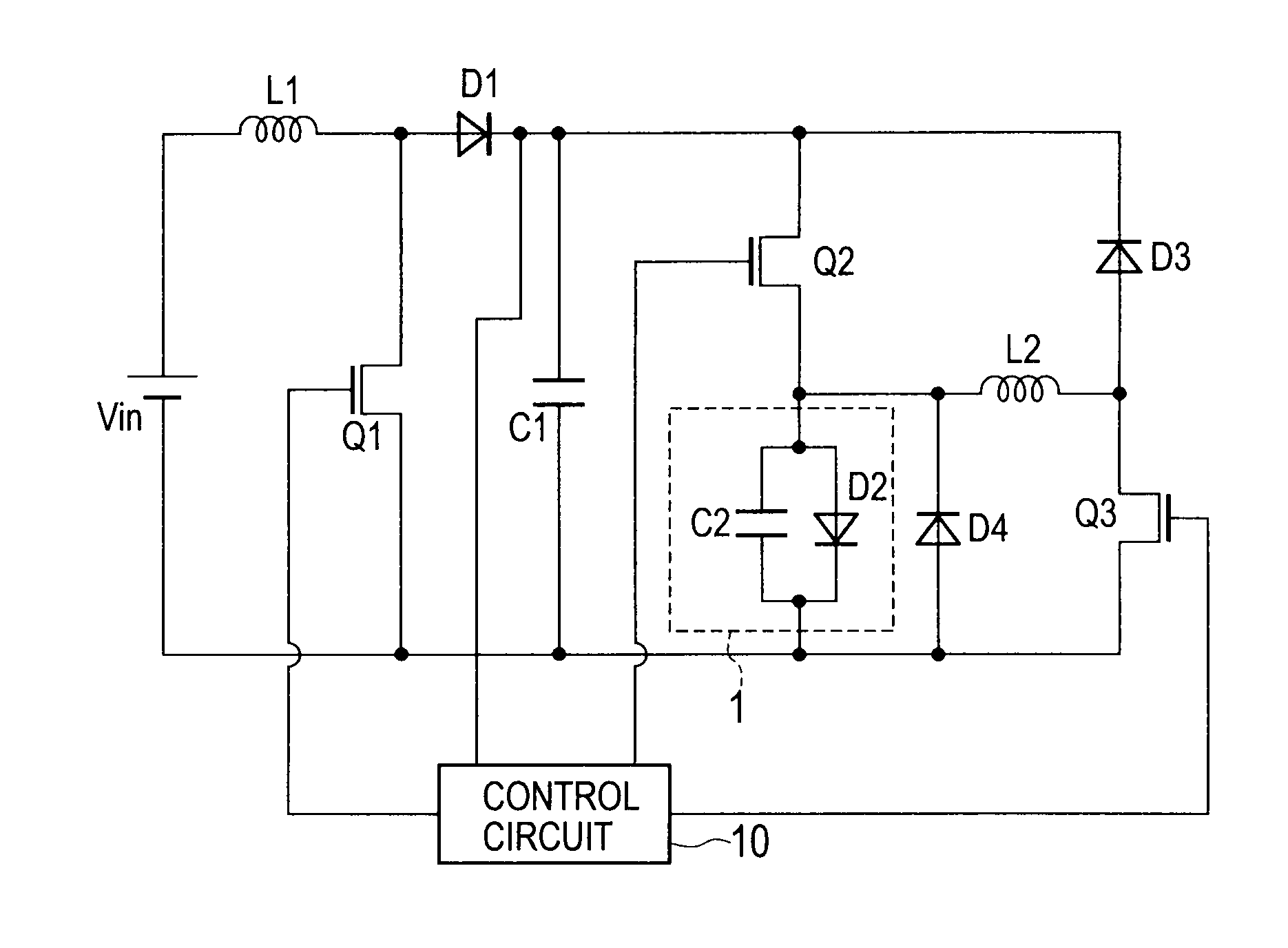
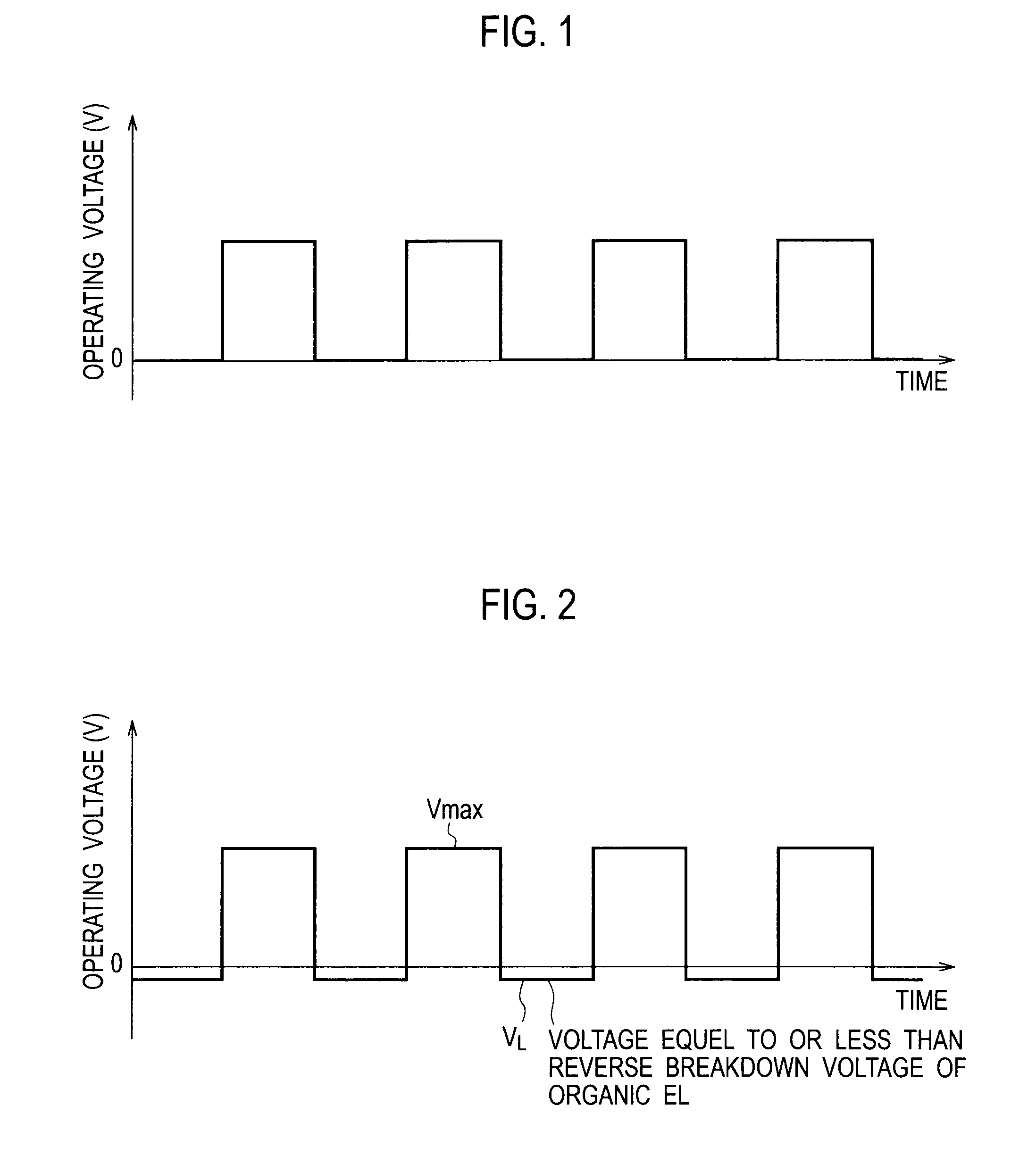
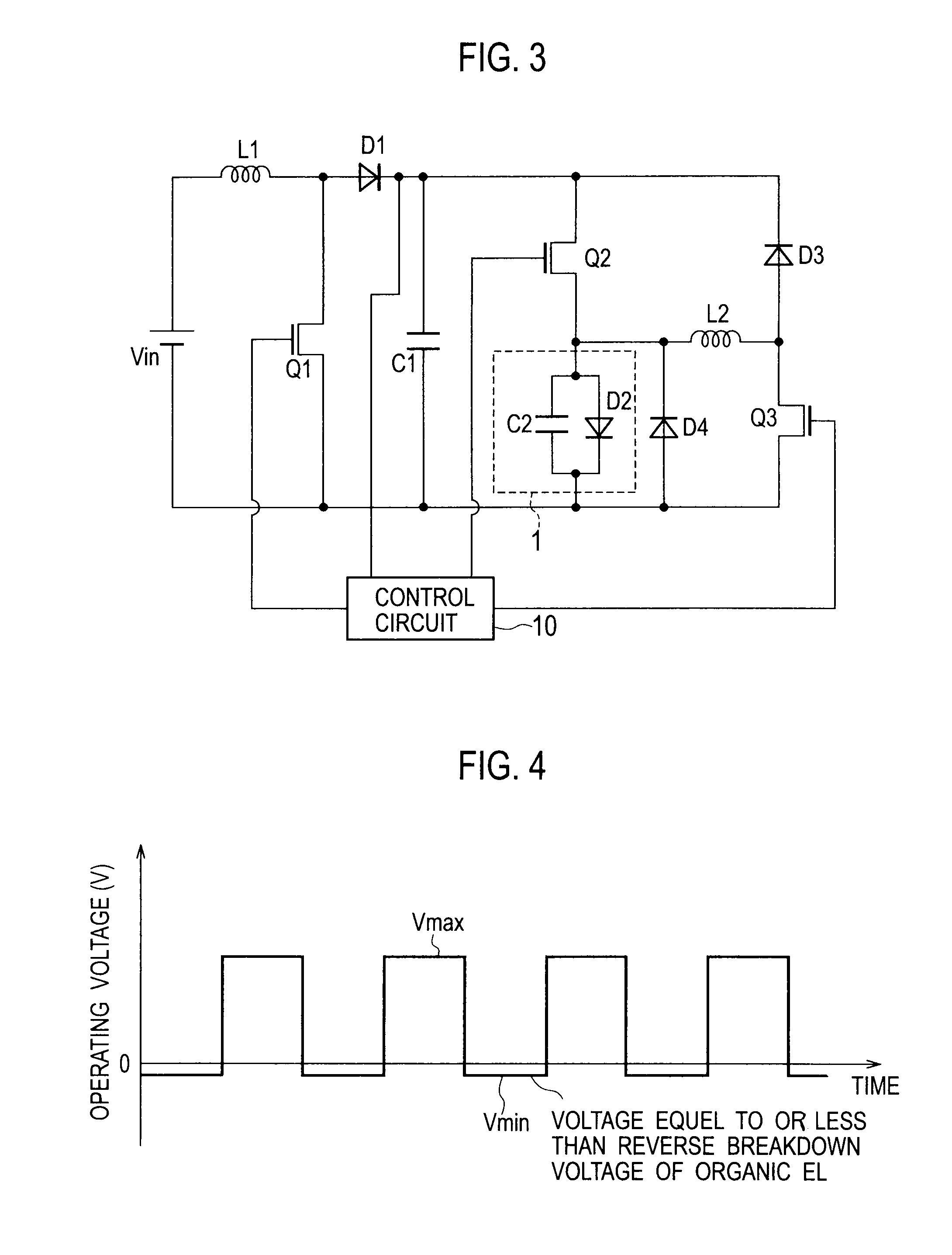
[0032]FIG. 3 is a circuit diagram of the apparatus for driving a capacitive light emitting device according to Example 1. The apparatus for driving a capacitive light emitting device according to Example 1 is configured in that: electric charges having been accumulated in the capacitive light emitting device are drawn out therefrom by applying a reverse bias voltage Vmin, which is equal to or less than a reverse breakdown voltage of the capacitive light emitting device, to the capacitive light emitting device as shown in FIG. 4; and the electric charges thus drawn-out are reused for light emission of the capacitive light emitting device after returned to the power supply for regeneration. This configuration makes it possible to extend the life of the capacitive light emitting device, and to use the electric power with high efficiency.
[0033]The capacitive light emitting device is a device which has a large capacitive component like organic EL devices each made of an organic substance...
example 2
[0052]FIG. 9 is a circuit diagram of an apparatus for driving a capacitive light emitting device according to Example 2. Example 2 is characteristic in that multiple capacitive light emitting devices 1 are independently controlled with one power supply.
[0053]The series circuit including the reactor L1 and the drive element Q1 made of the MOSFET is connected to the two ends of the DC power supply Vin. N series circuits are connected between the drain and source of the drive element Q1 in a way that: a series circuit including a drive element Q11 made of a MOSFET and a part 3-1 for driving a capacitive light emitting device is connected between the drain and source of the drive element Q1; and a series circuit including a drive element Q12 made of a MOSFET and a part 3-2 for driving a capacitive light emitting device is connected between the drain and source of the drive element Q1.
[0054]Each of the parts 3-1 to 3-n for driving the respective capacitive light emitting devices is confi...
example 3
[0057]FIG. 10 is a circuit diagram of an apparatus for driving a capacitive light emitting device according to Example 3. In FIG. 10, a capacitor C3 is connected to the two ends of the DC power supply Vin, and a series circuit including a drive element Q4 made of a MOSFET and a drive element Q5 made of a MOSFET is connected between the two ends of this capacitor C3. A diode D5 is connected between the drain and source of the drive element Q4, and a diode D6 is connected between the drain and source of the drive element Q5.
[0058]A series circuit including a reactor L3 and a diode D7 is connected to the two ends of the diode D6. The capacitive light emitting device 1 is connected to the two ends of the diode D7. A voltage reduced by a forward voltage drop of the diode D7 is equal to or less than the reverse breakdown voltage of the capacitive light emitting device 1.
[0059]A control circuit 11 is connected to the gate of the drive element Q4 and the gate of the drive element Q5, and th...
PUM
 Abstract
Description
Claims
Application Information
 - R&D Engineer
- R&D Manager
- IP Professional
- Industry Leading Data Capabilities
- Powerful AI technology
- Patent DNA Extraction
Browse by: Latest US Patents, China's latest patents, Technical Efficacy Thesaurus, Application Domain, Technology Topic.
© 2024 PatSnap. All rights reserved.Legal|Privacy policy|Modern Slavery Act Transparency Statement|Sitemap