Composite electronic device, manufacturing method thereof, and connection structure of composite electronic device

a composite electronic device and manufacturing method technology, applied in the direction of overvoltage protection resistors, fixed transformers or mutual inductances, emergency protective arrangements for limiting excess voltage/current, etc., can solve the problem of large esd (electrostatic discharge) problem, signal waveform becomes inert, circuit generates relatively large radiation electromagnetic field, etc. problem, to achieve the effect of small electrostatic capacitance, excellent discharge characteristic, heat resistance and weatherability

Active Publication Date: 2011-01-13
TDK CORPARATION
View PDF16 Cites 34 Cited by
  • Summary
  • Abstract
  • Description
  • Claims
  • Application Information

AI Technical Summary

Benefits of technology

[0027]As described above, according to the present invention, it is possible to provide a compact and high-performance composite electronic device constituted by combining a common mode filter and ESD protection elements having a small electrostatic capacitance and excellent discharge characteristic, heat resistance, and weatherability. Particularly, the composite electronic device

Problems solved by technology

However, this circuit generates a relatively large radiation electromagnetic field when common noise (common mode noise) is superimposed on the signal lines 1 and 2.
Accordingly, ESD (electrostatic discharge) becomes a large problem.
However, when the varistor is used, a signal waveform becomes inert, and signal quality is degraded.
Therefore, the ESD prot

Method used


Image

  • Composite electronic device, manufacturing method thereof, and connection structure of composite electronic device
  • Composite electronic device, manufacturing method thereof, and connection structure of composite electronic device
  • Composite electronic device, manufacturing method thereof, and connection structure of composite electronic device

Examples


first embodiment

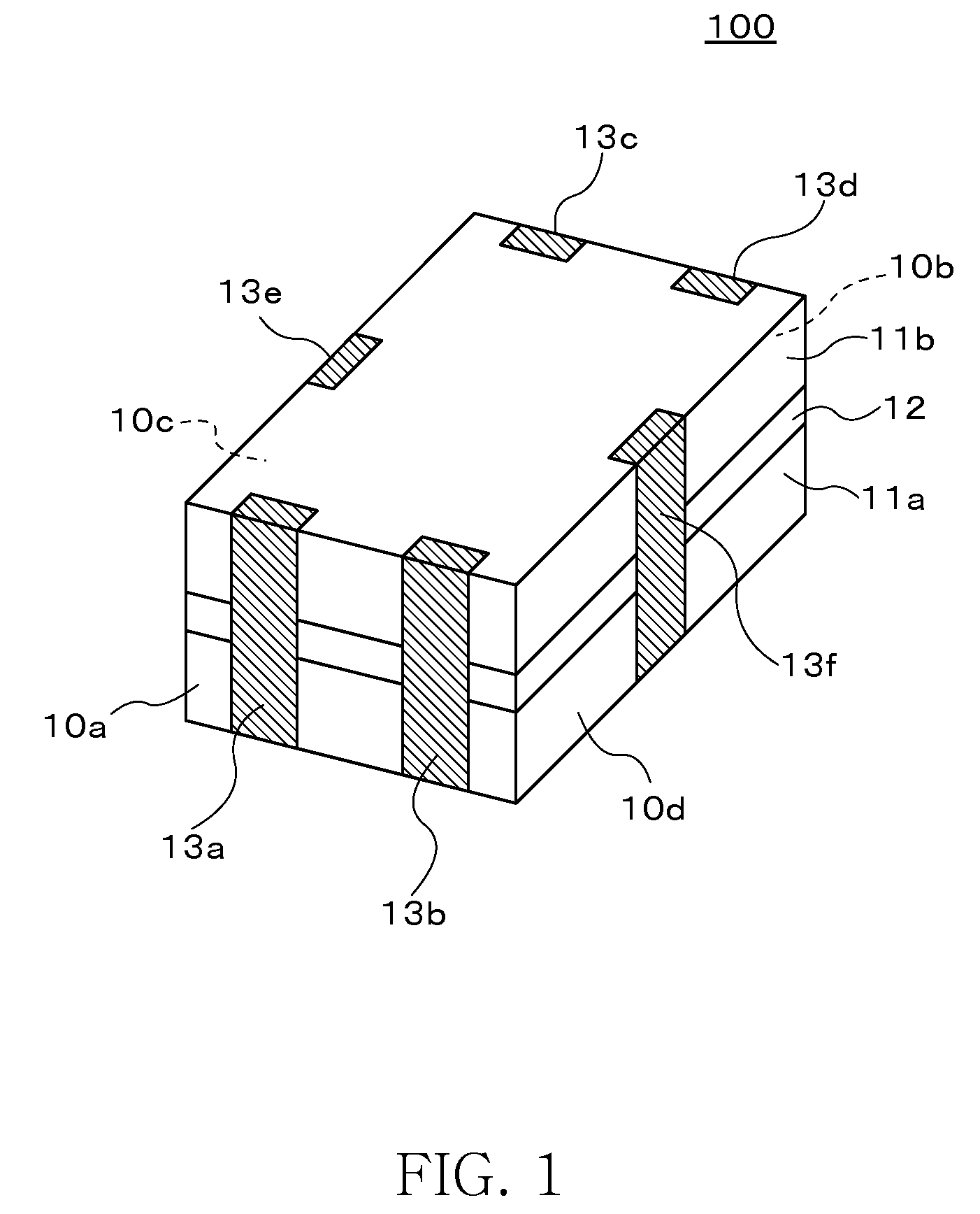
[0046]FIG. 1 is a schematic perspective view showing an external configuration of a composite electronic device according to the present invention.

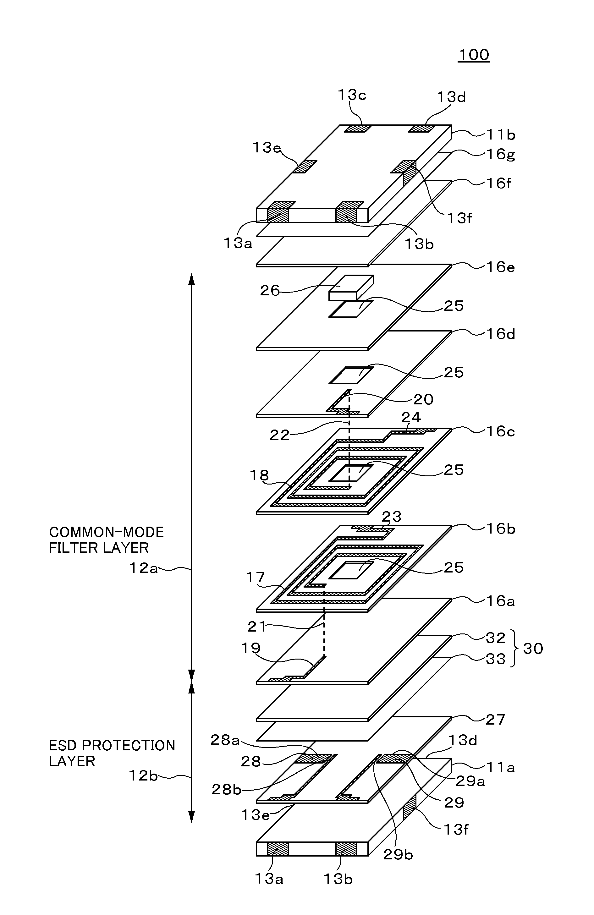
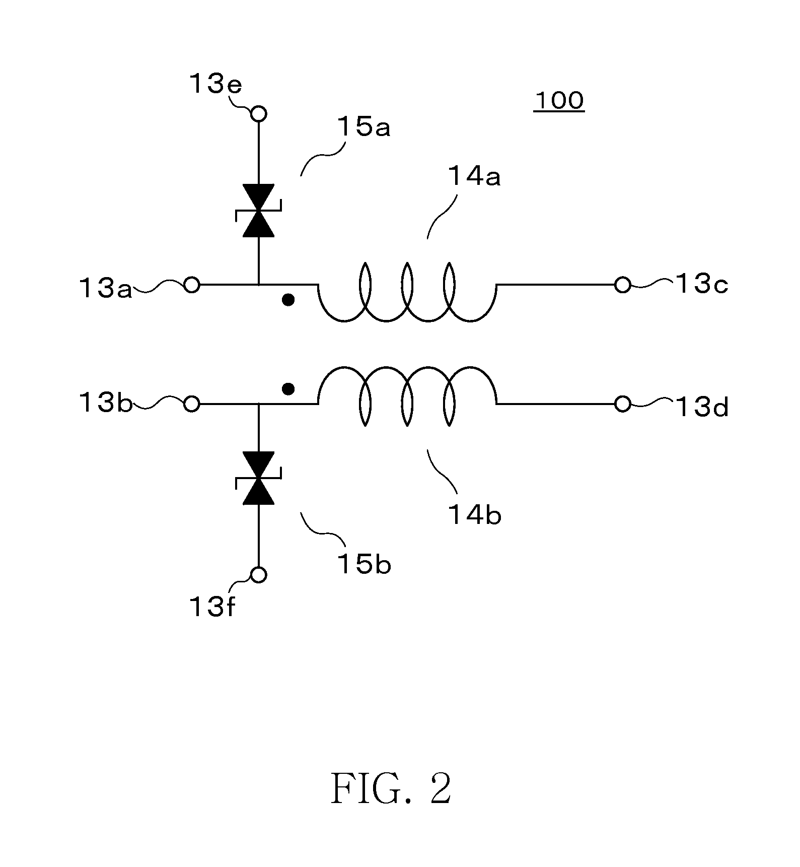
[0047]As shown in FIG. 1, a composite electronic device 100 according to the first embodiment is a thin-film common mode filter having an ESD protection function, and includes first and second magnetic substrates 11a and 11b, and a function layer 12 sandwiched between the first magnetic substrate 11a and the second magnetic substrate 11b. First to sixth terminal electrodes 13a to 13f are formed on an external peripheral circuit of a laminated body constituted by the first magnetic substrate 11a, the function layer 12, and the second magnetic substrate 11b. The first and second terminal electrodes 13a and 13b are formed on a first side surface 10a. The third and fourth terminal electrodes 13c and 13d are formed on a second side surface 10b opposite to the first side surface 10a. The fifth terminal electrode 13e is formed on a third side su...

second embodiment

[0102]FIG. 9 is a schematic perspective view showing a layer structure of a composite electronic device 200 according to the present invention.

[0103]As shown in FIG. 9, in the composite electronic device 200, the first and second lead conductors 19 and 20 of the common-mode filter layer 12a are formed on the common insulation layer 16a. Therefore, the insulation layer formed with the second lead conductor 20 in the first embodiment is omitted, and one insulation layer becomes unnecessary. Consequently, a layer thickness of the common-mode filter layer 12a can be reduced, and the composite electronic device 200 can have a small height, and a manufacturing step thereof can be simplified.

third embodiment

[0104]FIG. 10 is a schematic perspective view showing a layer structure of a composite electronic device 300 according to the present invention.

[0105]As shown in FIG. 10, in the composite electronic device 300, the common-mode filter layer 12a is provided on a lower layer, and the ESD protection layer 12b is provided on an upper layer. Because there is no change in the configuration of the common-mode filter layer 12a and in the configuration of the ESD protection layer 12b, like constituent elements are denoted by like reference characters, and redundant explanations thereof will be omitted. According to the third embodiment, the composite electronic device 300 includes low-voltage type ESD protection elements having a small electrostatic capacitance, a low discharge starting voltage, and excellent discharge resistance, heat resistance, and weatherability, in a similar manner to that of the first embodiment. Therefore, a composite electronic device functioning as a common mode filt...


PUM

PropertyMeasurementUnit
Capacitanceaaaaaaaaaa
Electrical conductoraaaaaaaaaa
Magnetismaaaaaaaaaa

Abstract

The present invention is provided with a composite electronic device comprising an inductor element and an ESD protection element formed between two magnetic substrates, wherein the inductor element includes insulation layers made of a resin, and conductor patterns formed on the insulation layers, the ESD protection element includes a base insulation layer, a pair of electrodes arranged via gap formed therebetween on the base insulation layer, and an ESD absorbing layer arranged at least between the electrodes, and the ESD absorbing layer includes a composite material having an insulation inorganic material and a conductive inorganic material discontinuously dispersed in a matrix of the insulation inorganic material.

Description

TECHNICAL FIELD[0001]The present invention relates to a composite electronic device and a manufacturing method thereof, and, more particularly relates to a structure of a composite electronic device constituted by combining inductor elements and electrostatic discharge (ESD) protection elements. The present invention also relates to a structure of connection between such a composite electronic device and signal lines.BACKGROUND OF THE INVENTION[0002]In recent years, standards of USB 2.0 and a high-definition multimedia interface (HDMI) have been widely distributed as high-speed signal transmission interfaces, and they are used in many digital devices such as personal computers and digital high-vision televisions. These interfaces employ a differential signal system that transmits a differential signal (a differential mode signal) by using a pair of signal lines, unlike a single-end transmission system that has been generally used for many years.[0003]The differential transmission sy...

Claims


Application Information

Patent Timeline
IPC IPC(8): H02H9/00H02H3/22H05K3/44
CPCH01F17/0006H01F19/00H01T4/08H03H7/0107Y10T29/49124H05K1/0254H05K1/165H05K3/4629H03H7/427H03H2001/0085
Inventor ITO, TOMOKAZUHIROBE, YASUHIROHITOMI, ATSUSHITERADA, YUJIASAKURA, KENSAKUURANO, TAKESHI
Owner TDK CORPARATION
Why Eureka
Try Eureka